Zerocat Chipflasher: Kit User Guide
Chipflasher v2, assembled from scratch
Documentation for “Zerocat Chipflasher: Kit User Guide”
Generated on: Sun, 07 Dec 2025 11:29:21 +0100
Repository: git://zerocat.org/zerocat/projects/chipflasher.git
Board: board-v2.2.0-40-7362f65a7
Version: v2.3.0-356-7362f65a7
Branch: master
Chipflasher v2, assembled from scratch
Chipflasher v2 Kits
PCBs
Components
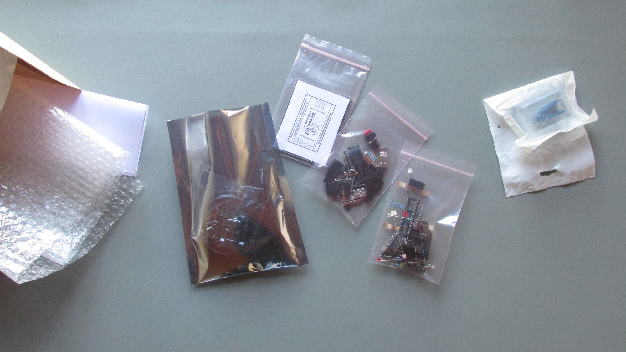
Kit: Scope of delivery
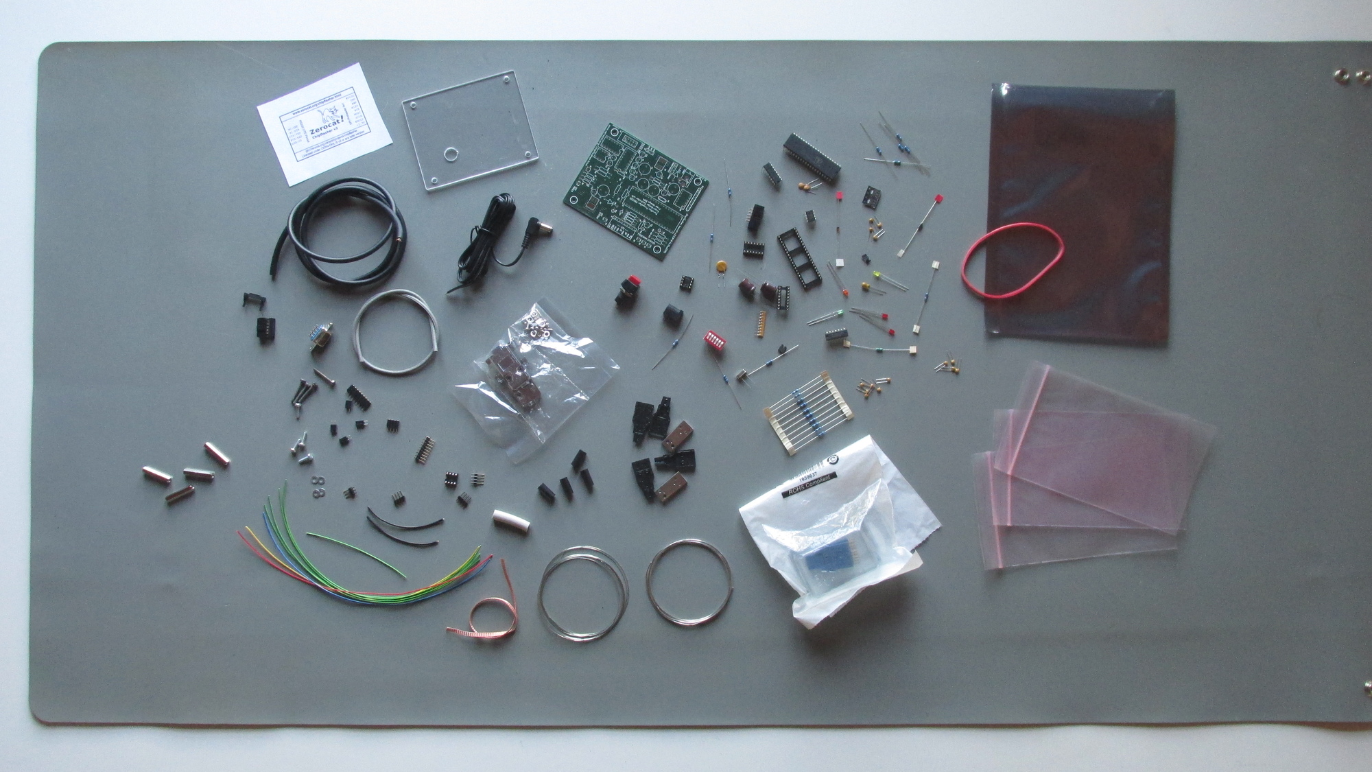
Kit: Bags purged
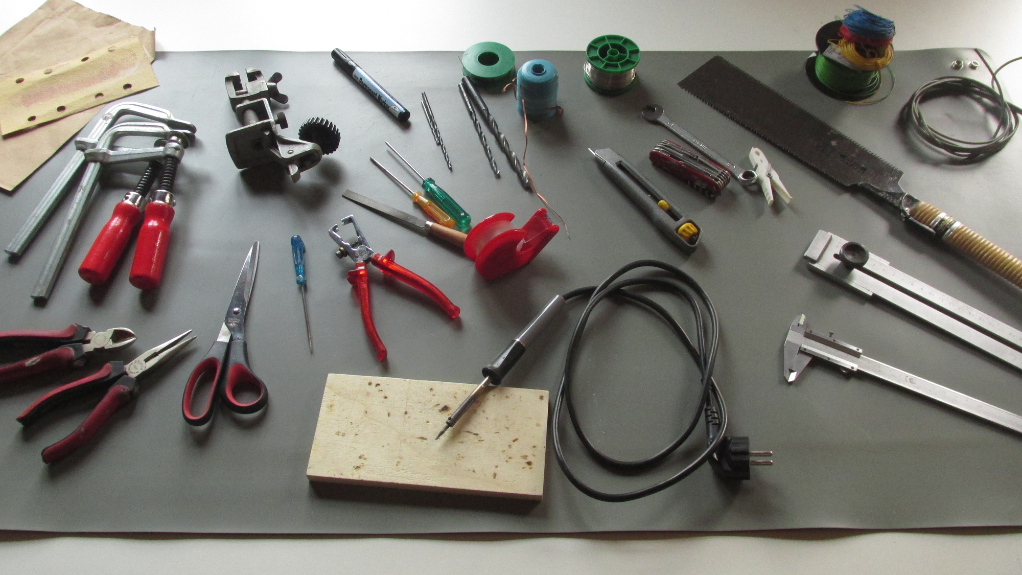
Set of Tools: Solder Iron and Accessories
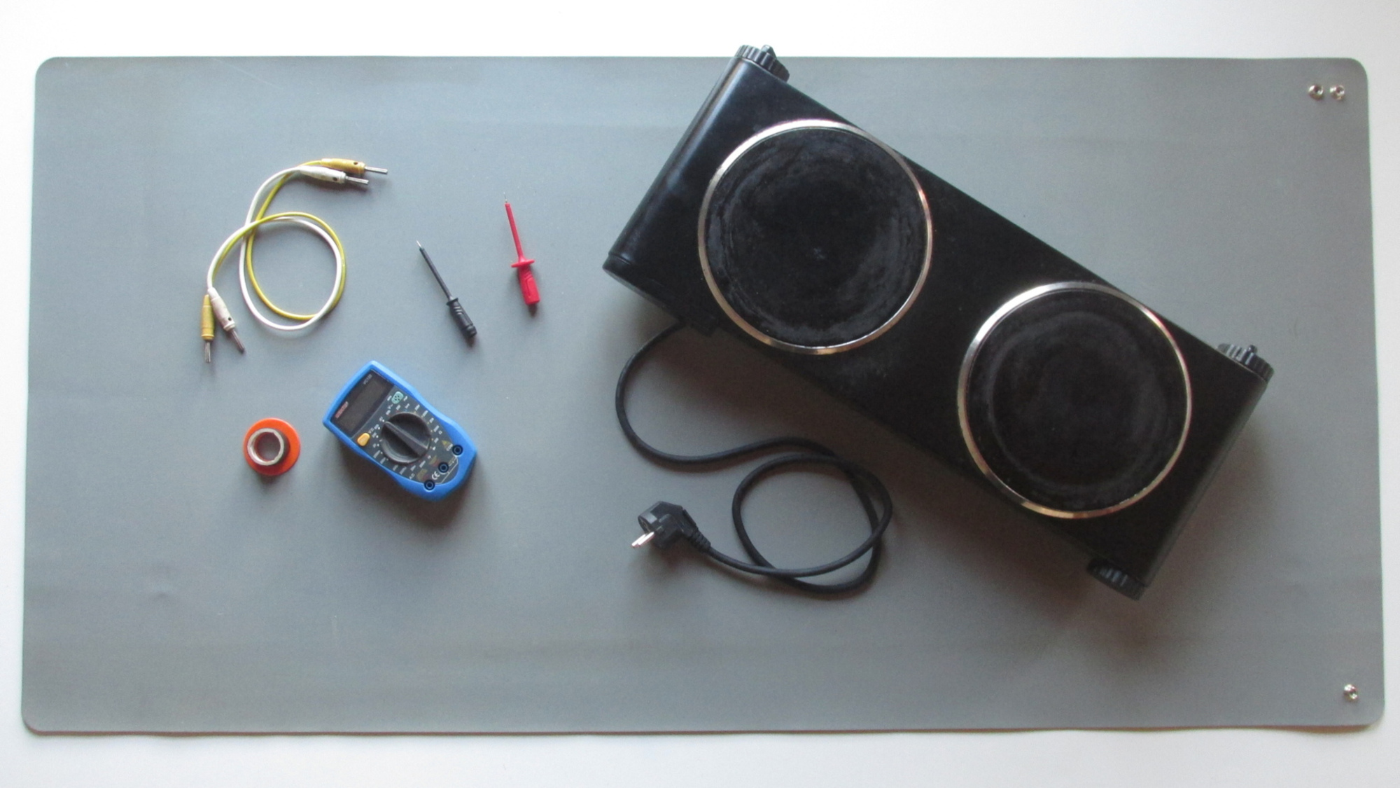
Set of Tools: Probe and Cooking Plate
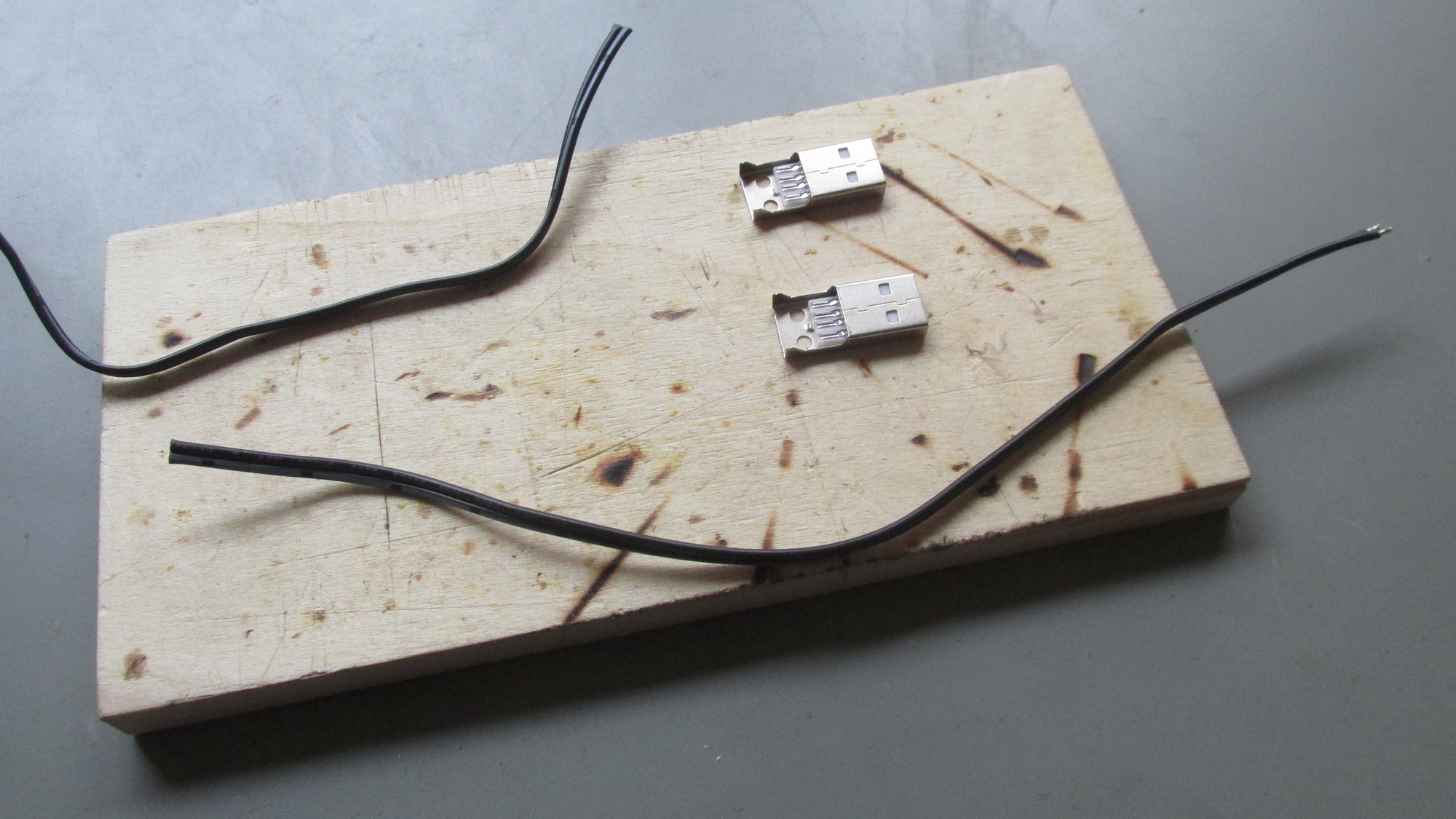
Cut like 20cm of Power Cable and get prepared: Locate wires marked with white stripes
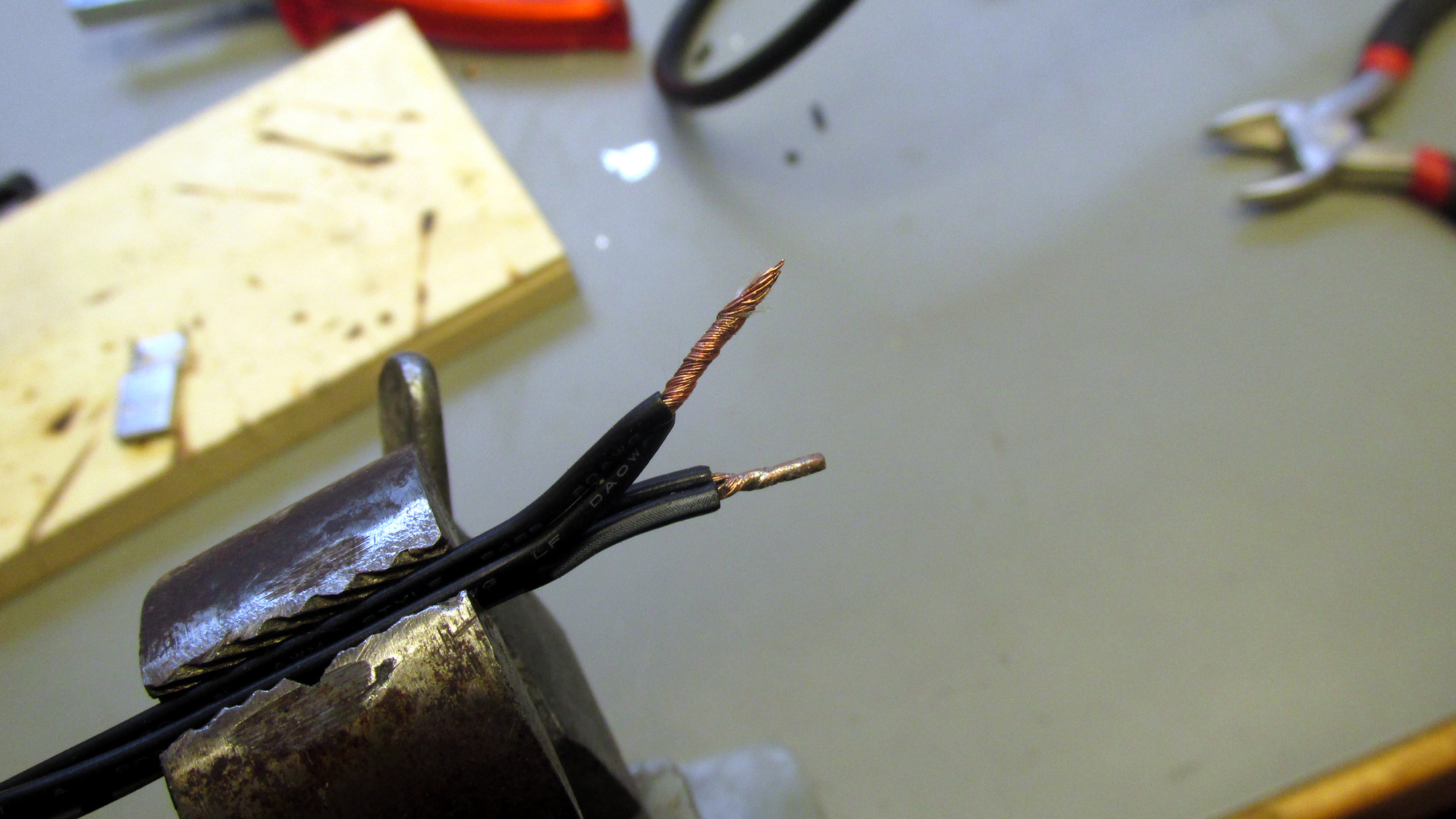
Join marked wires, join black wires, apply solder, grind joints to make them narrow
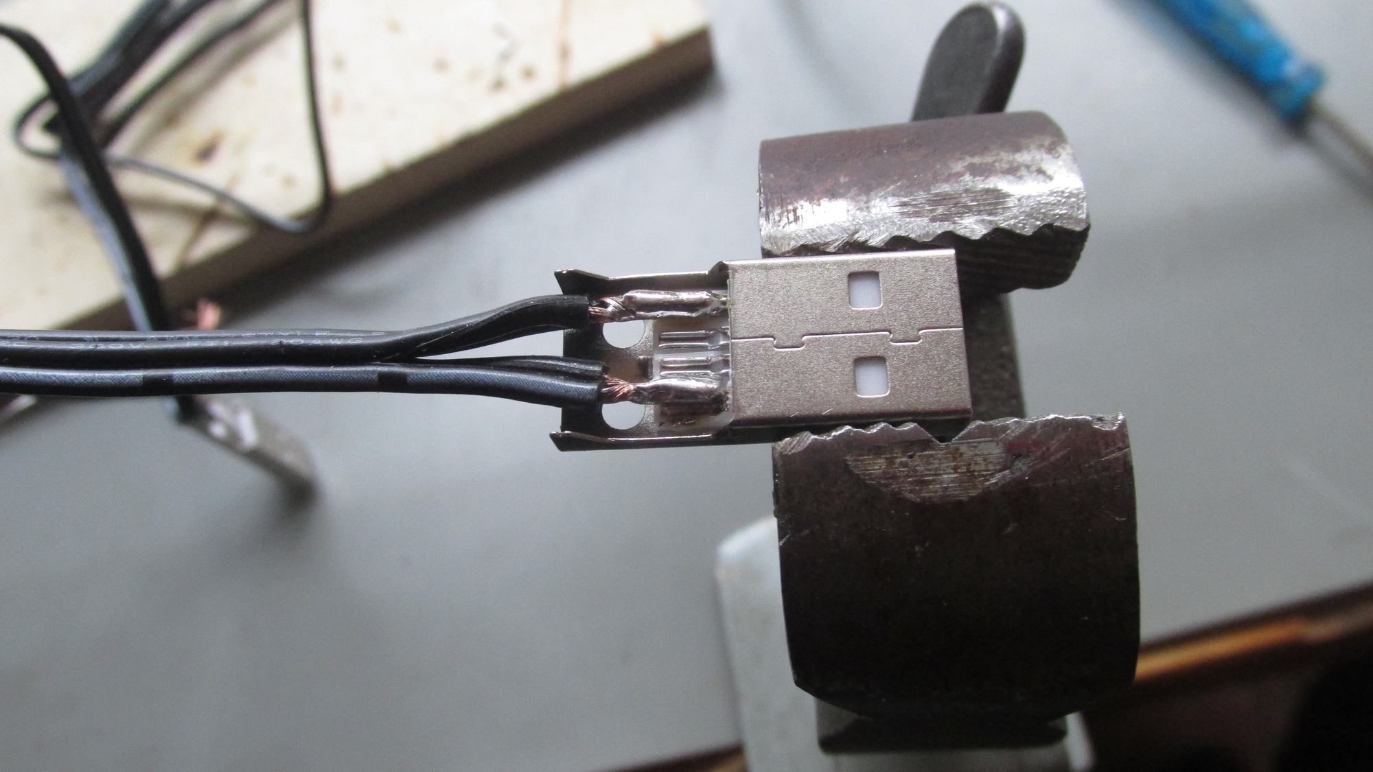
Solder plug, use marked wires for lower, 5VDC contact; avoid short circuits to data pins and chassis
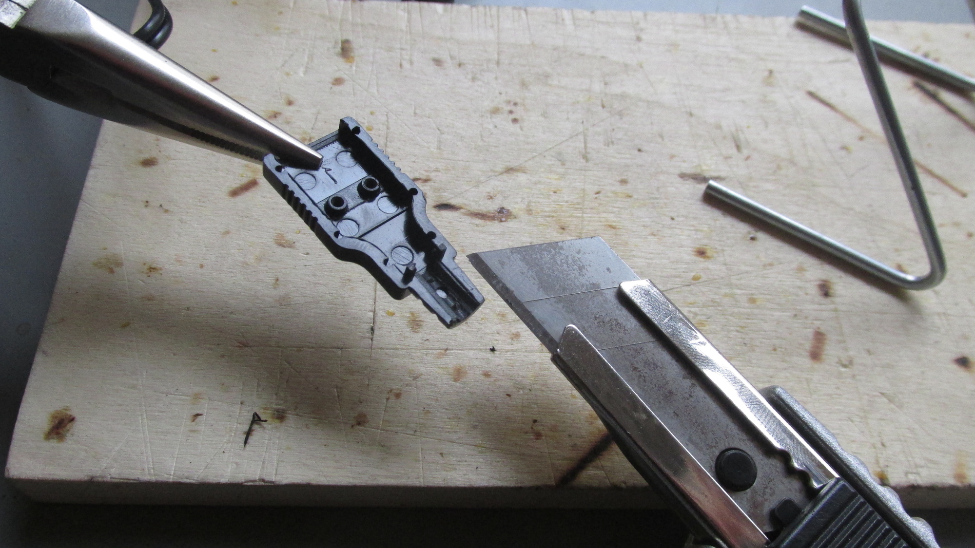
Cut handle to provide more space for quadruple wires
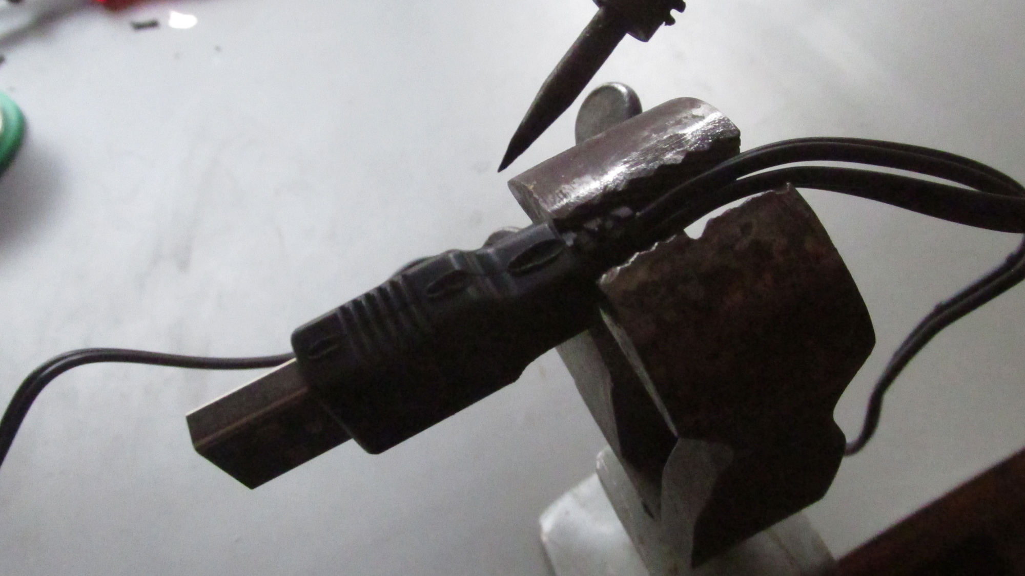
Place plug into handle, seal plastics with hot tip, then grind handle to make it look nice again
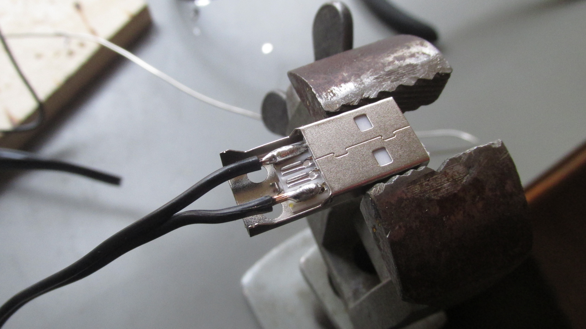
Solder second plug to remaining end of short power cable, again use marked wire for lower, 5VDC contact

Place plug into plastic handle, seal it again with hot tip
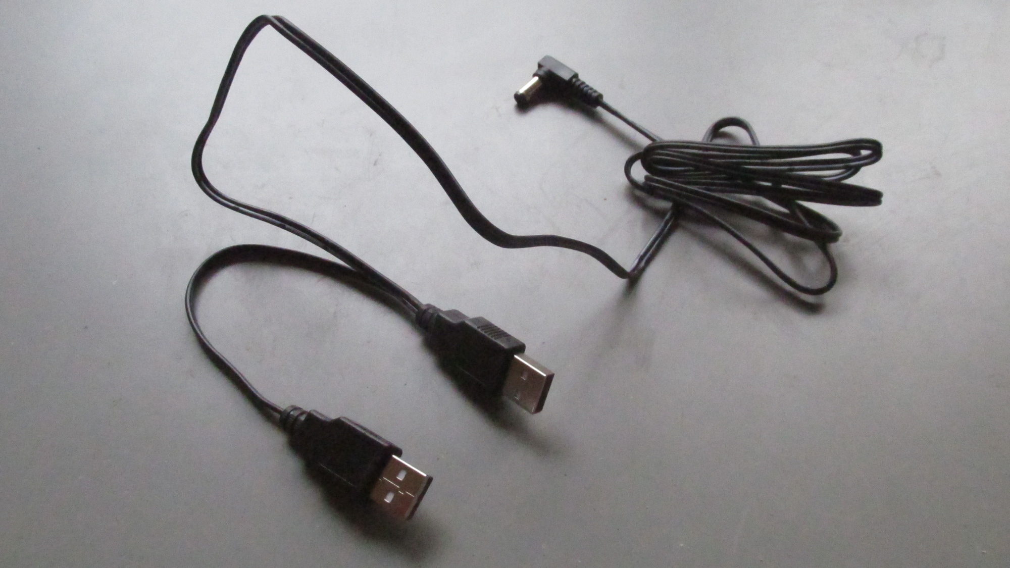
Done.
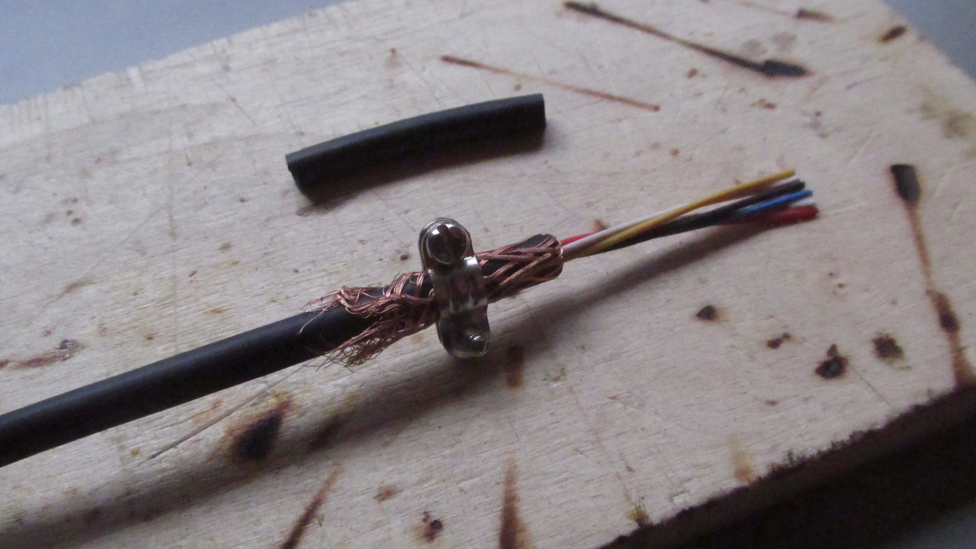
Take data cable, dismantel like 4cm and mount cable stop.
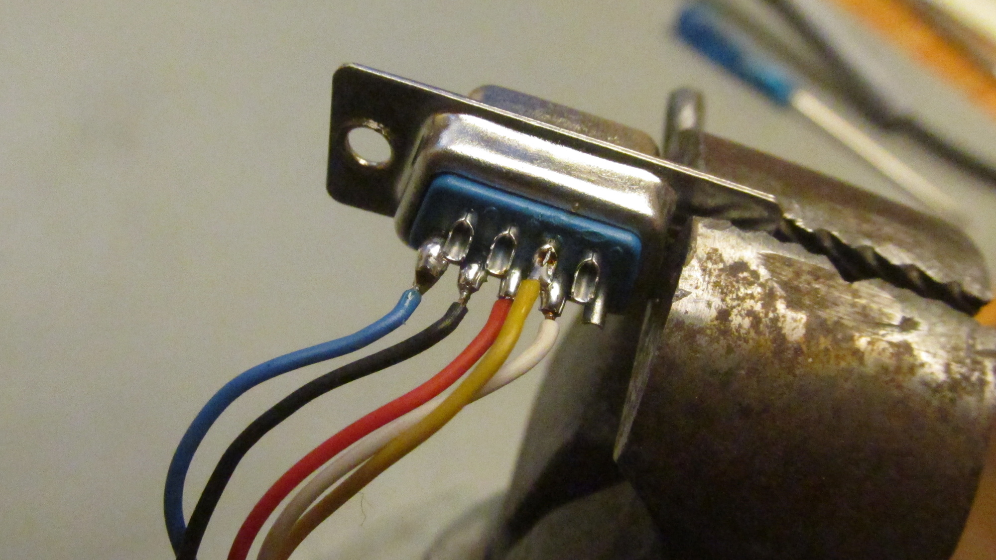
Solder wires, maintain color codes.
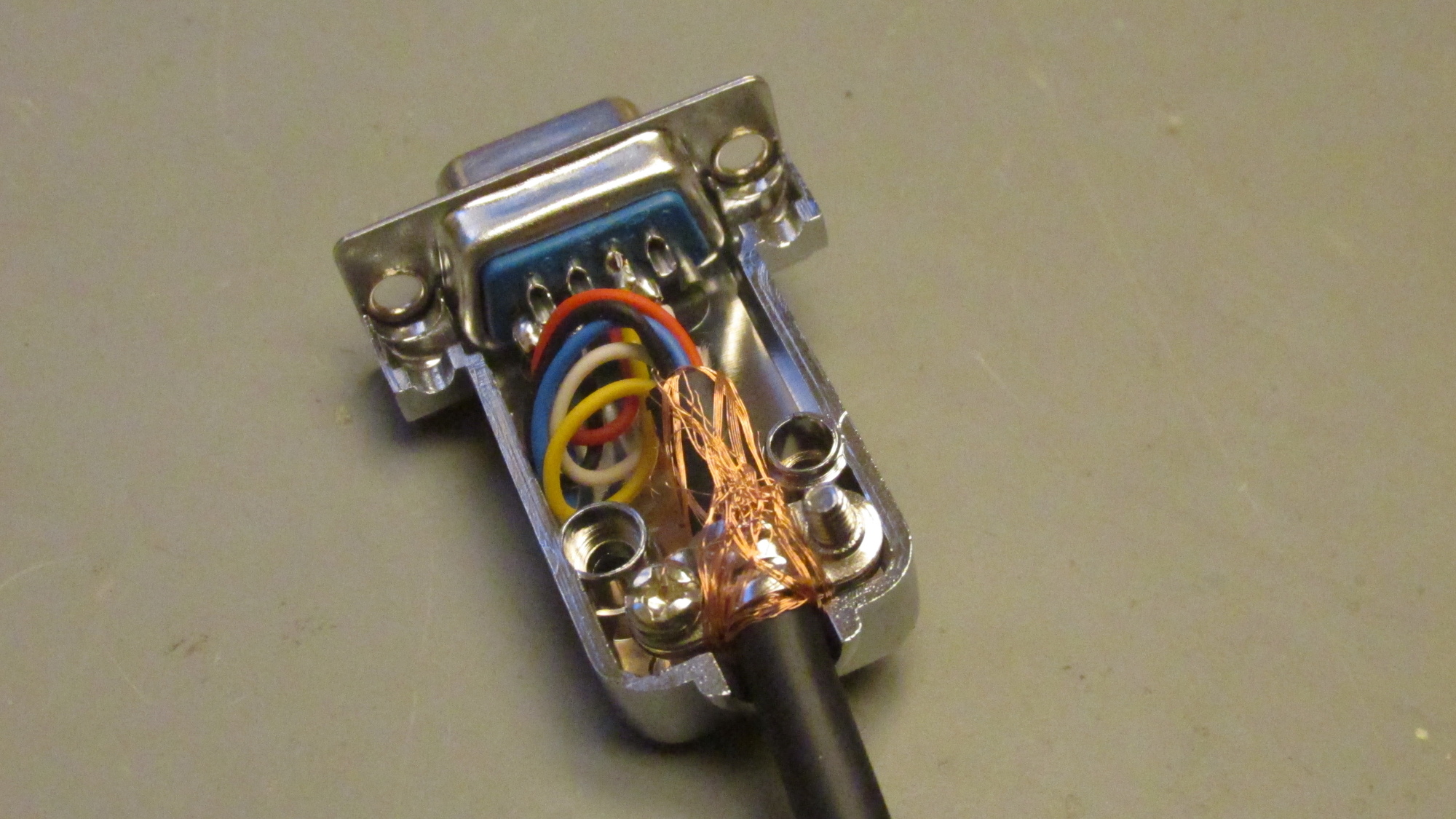
Mount plug handles.
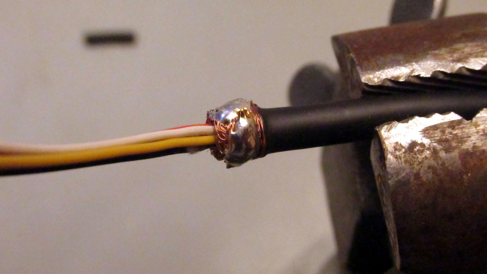
Other end of cable: Dismantel like 3cm, push back shield and seal with solder.
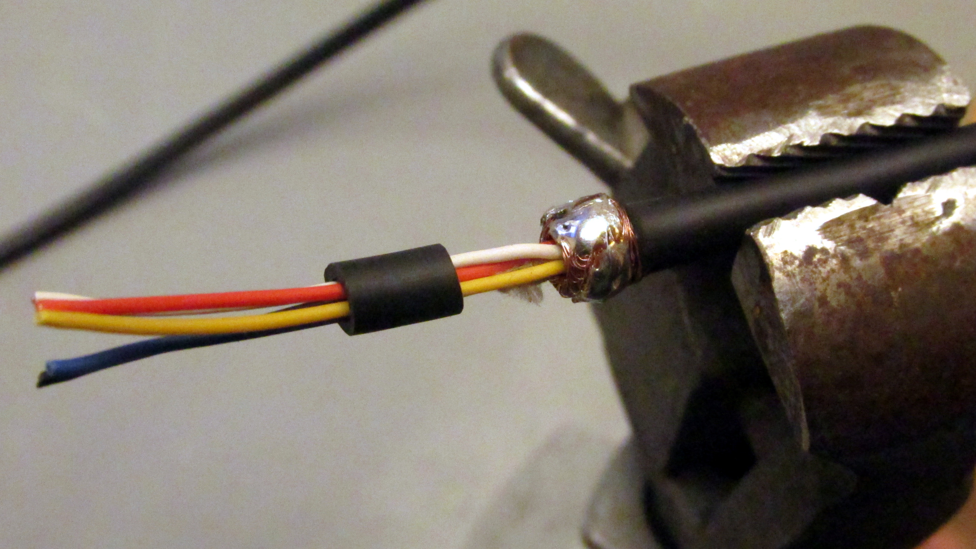
Add a small piece of mantel.
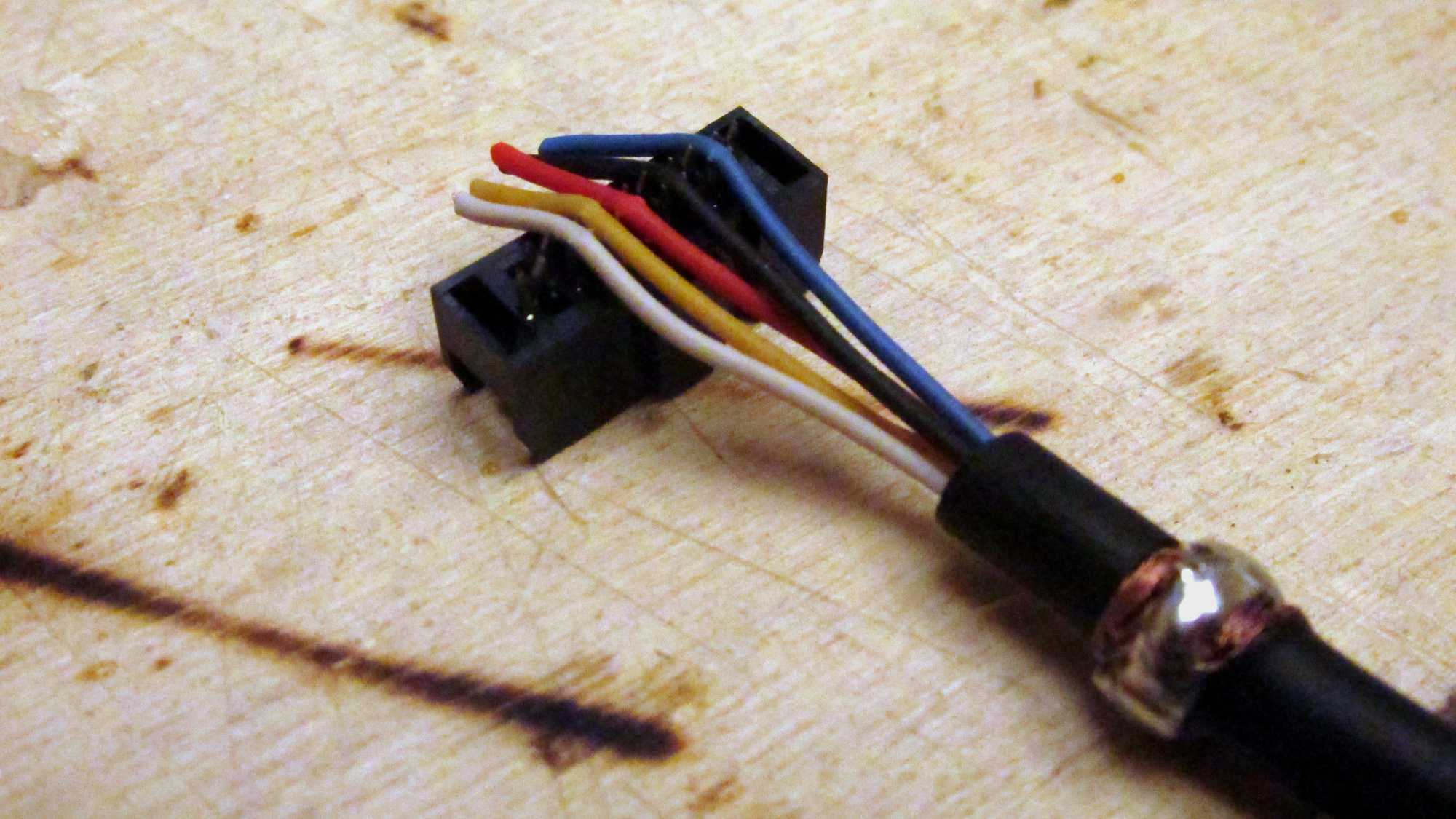
Press wires into plug.
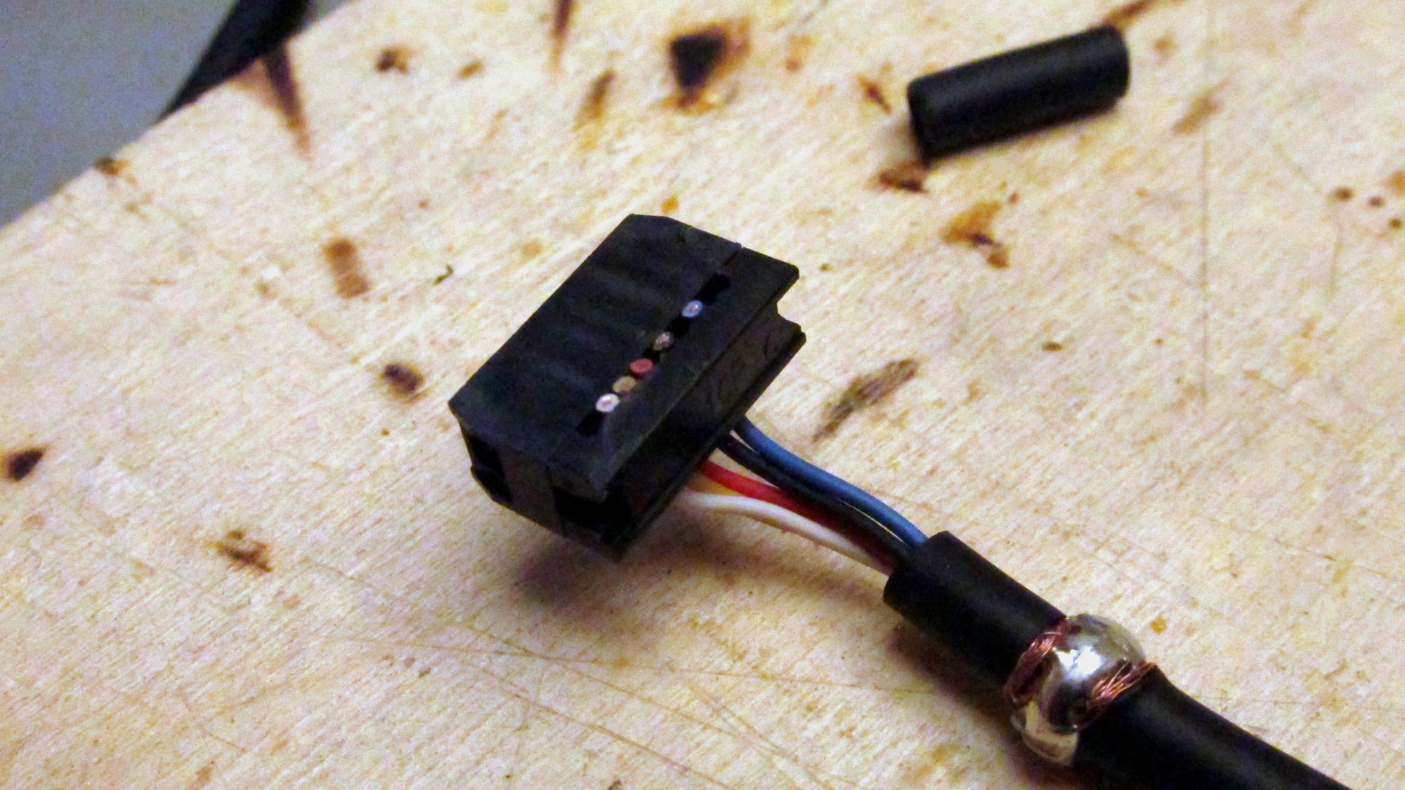
Close plug, cut in excess wires.
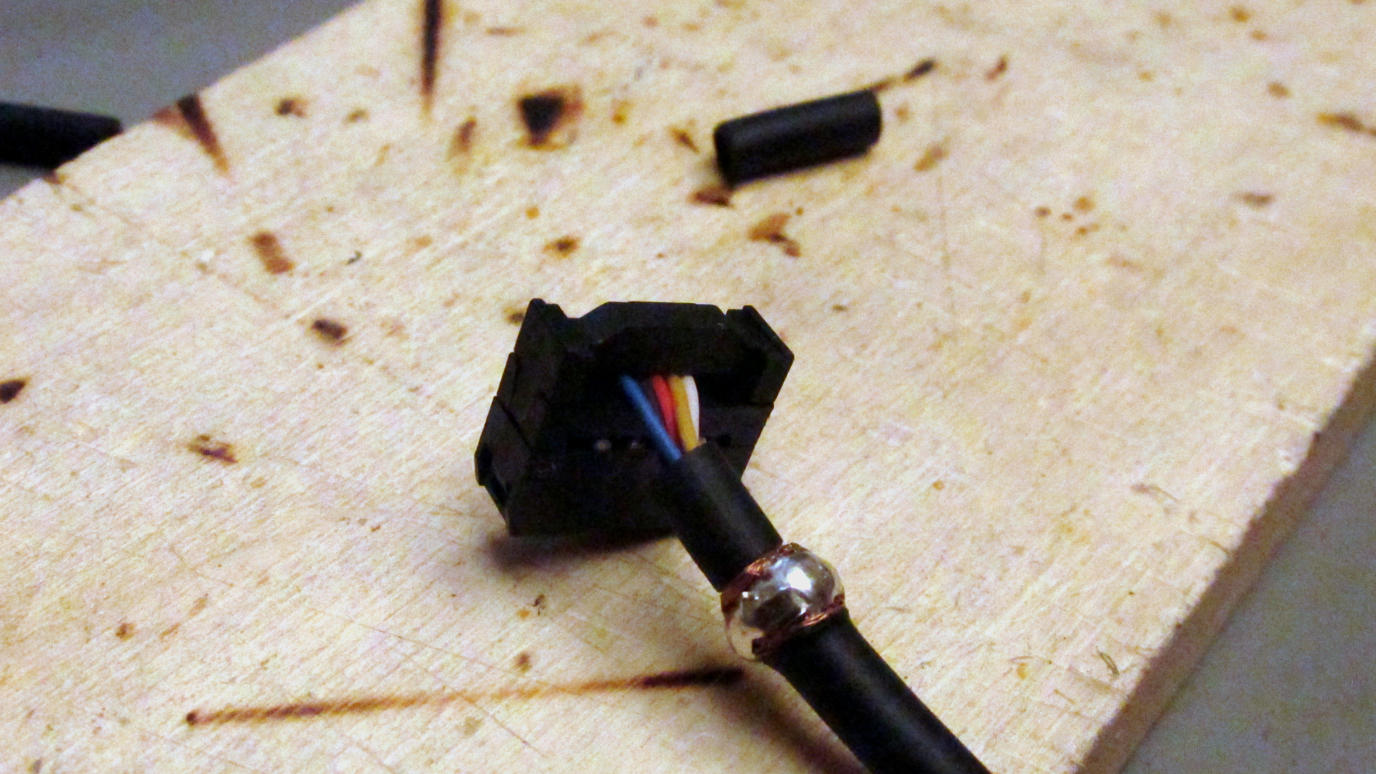
Finalize plug by adding cable stop.
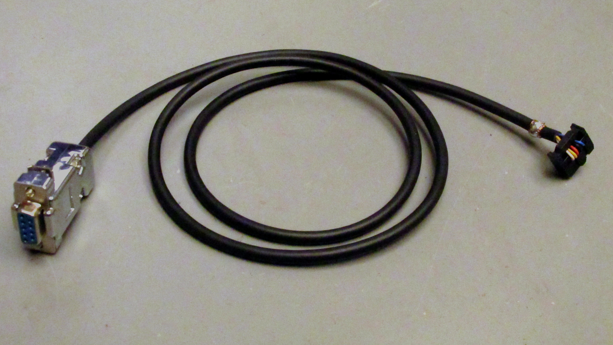
Done.
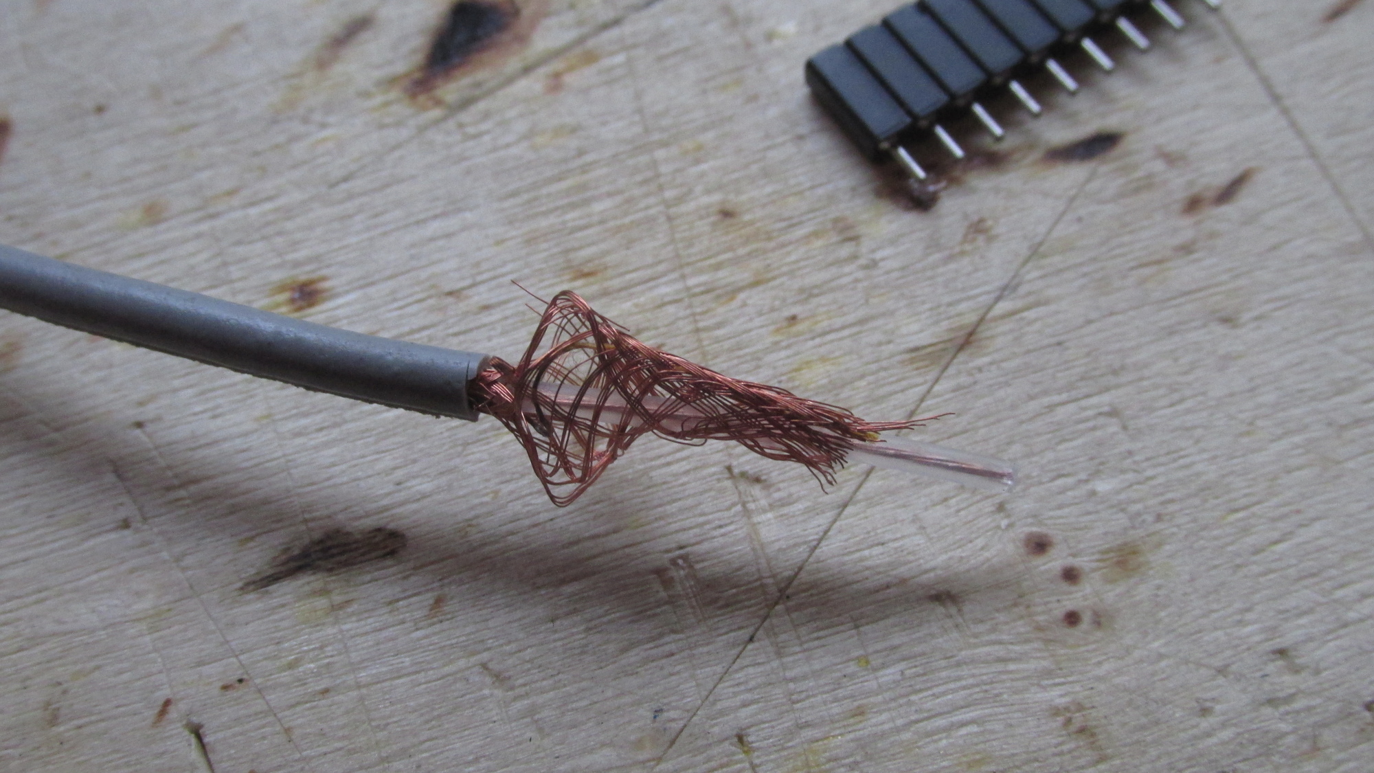
Get started: Dismantel like 3cm of shielded clock cable.
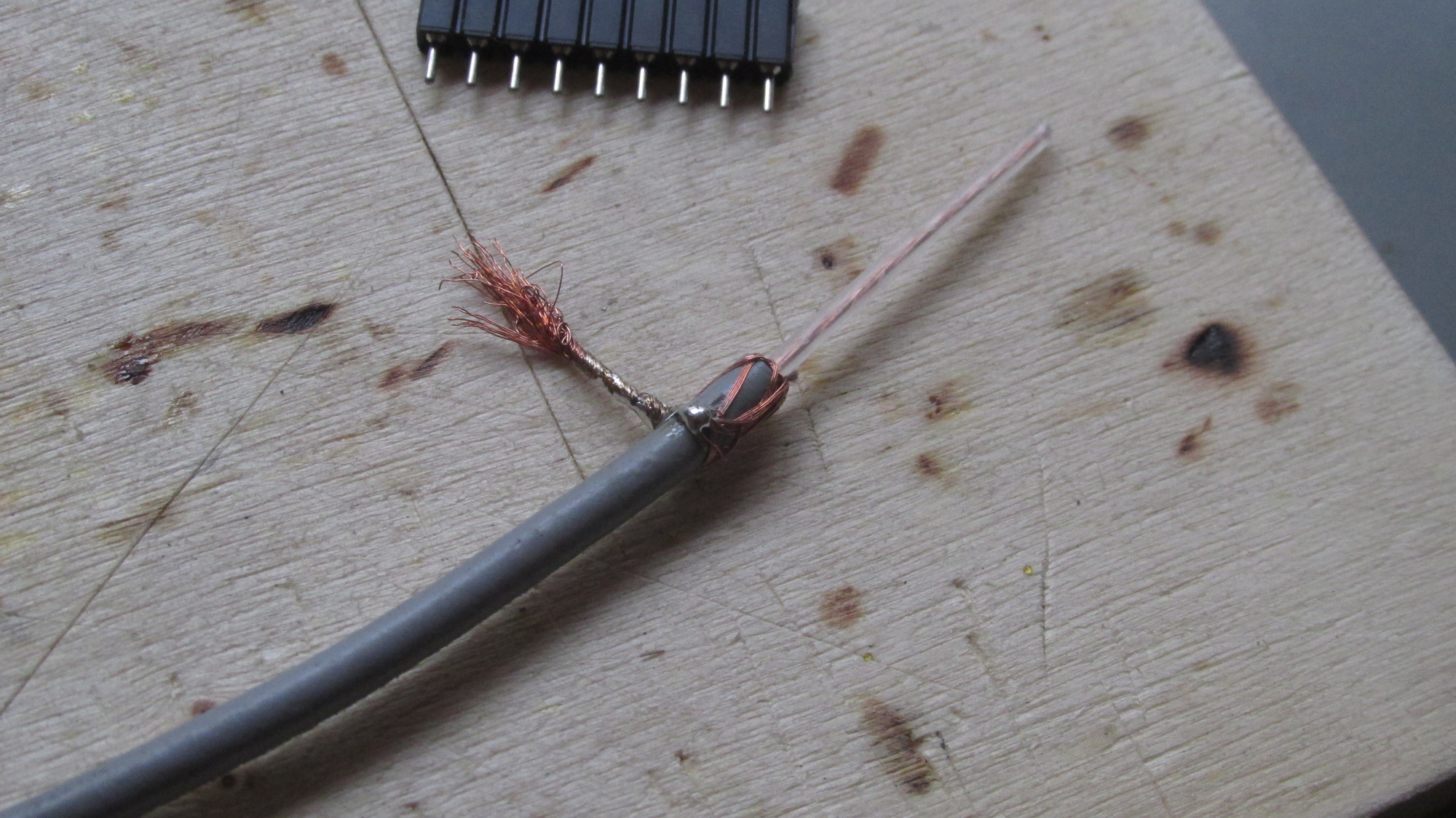
Push back shield, twist, apply solder.
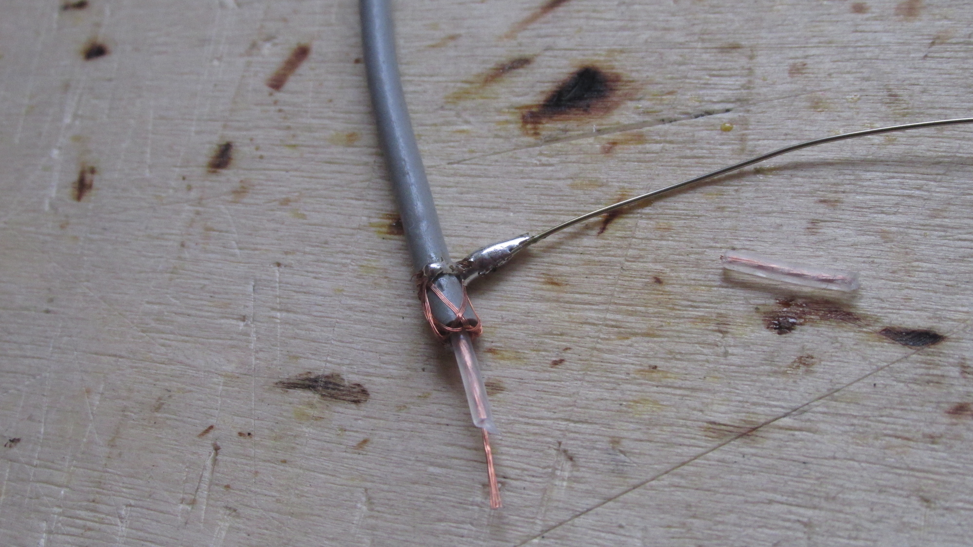
Dismantel clock wire, lenghten shield extension.
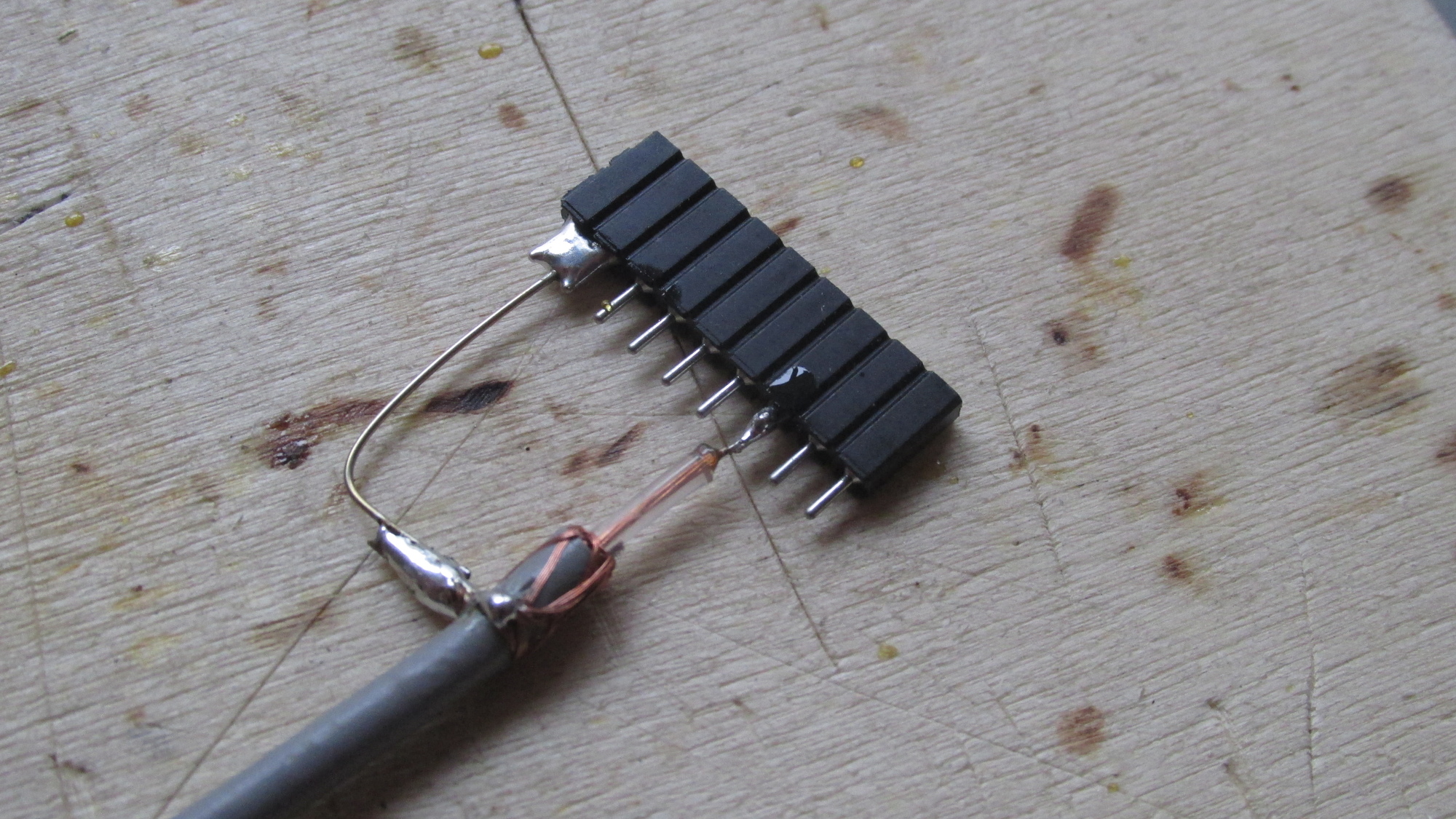
Connect clock wire and shield to 9×1 pinheader plug.
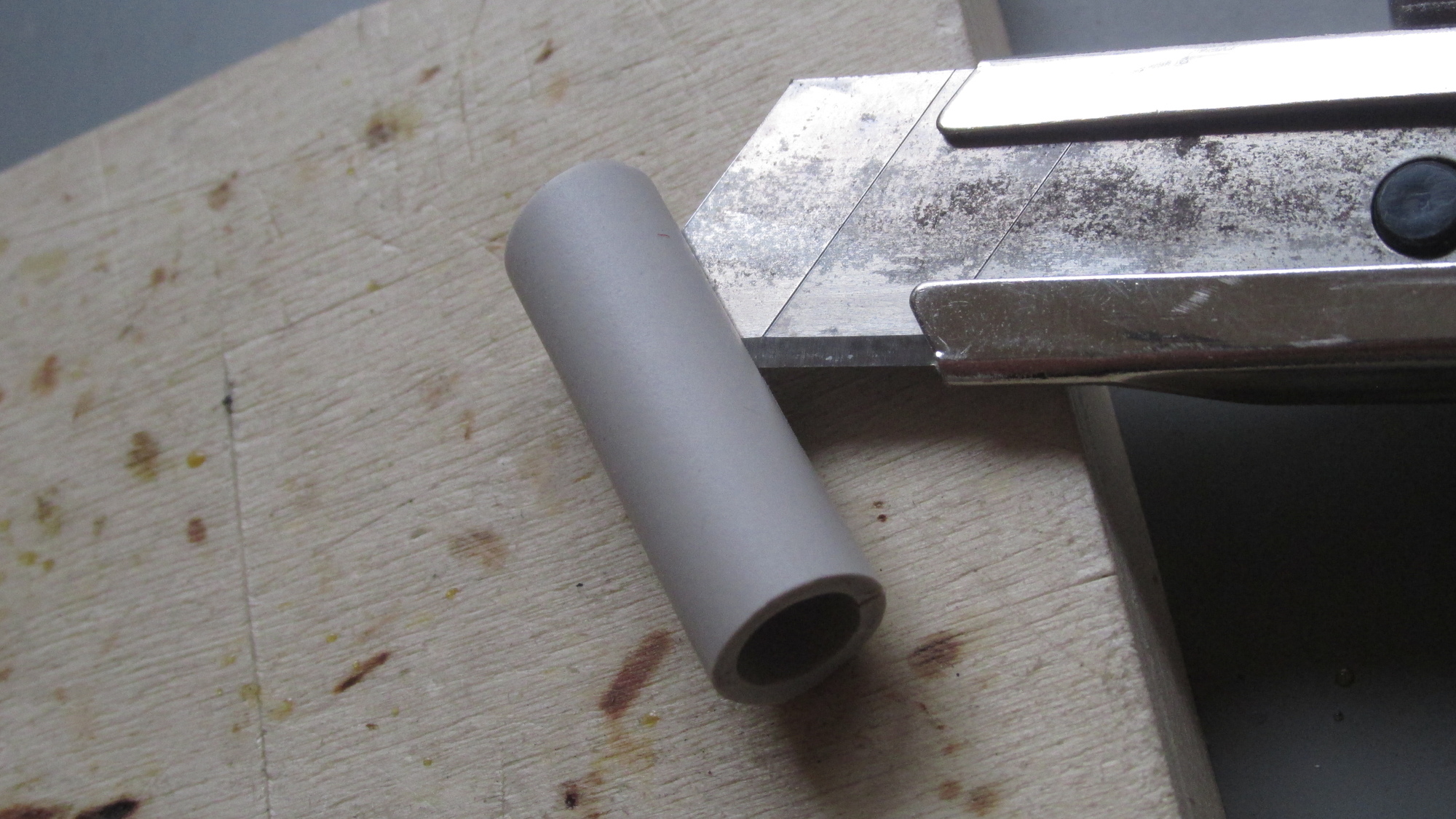
Cut gray piece of tube.
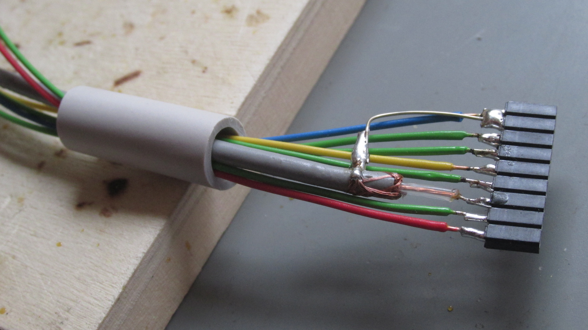
Add all missing wires while preserving color codes, bundle wires with tube.
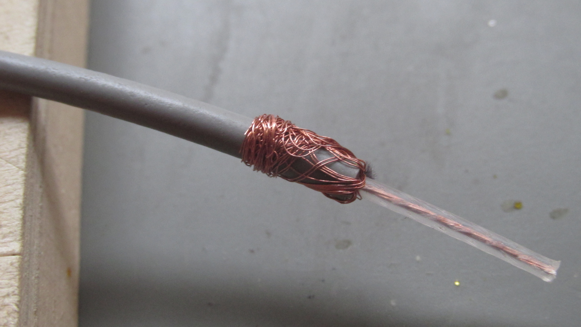
Other end of clock cable: Dismantel like 2cm, prepare shield for dead-end.
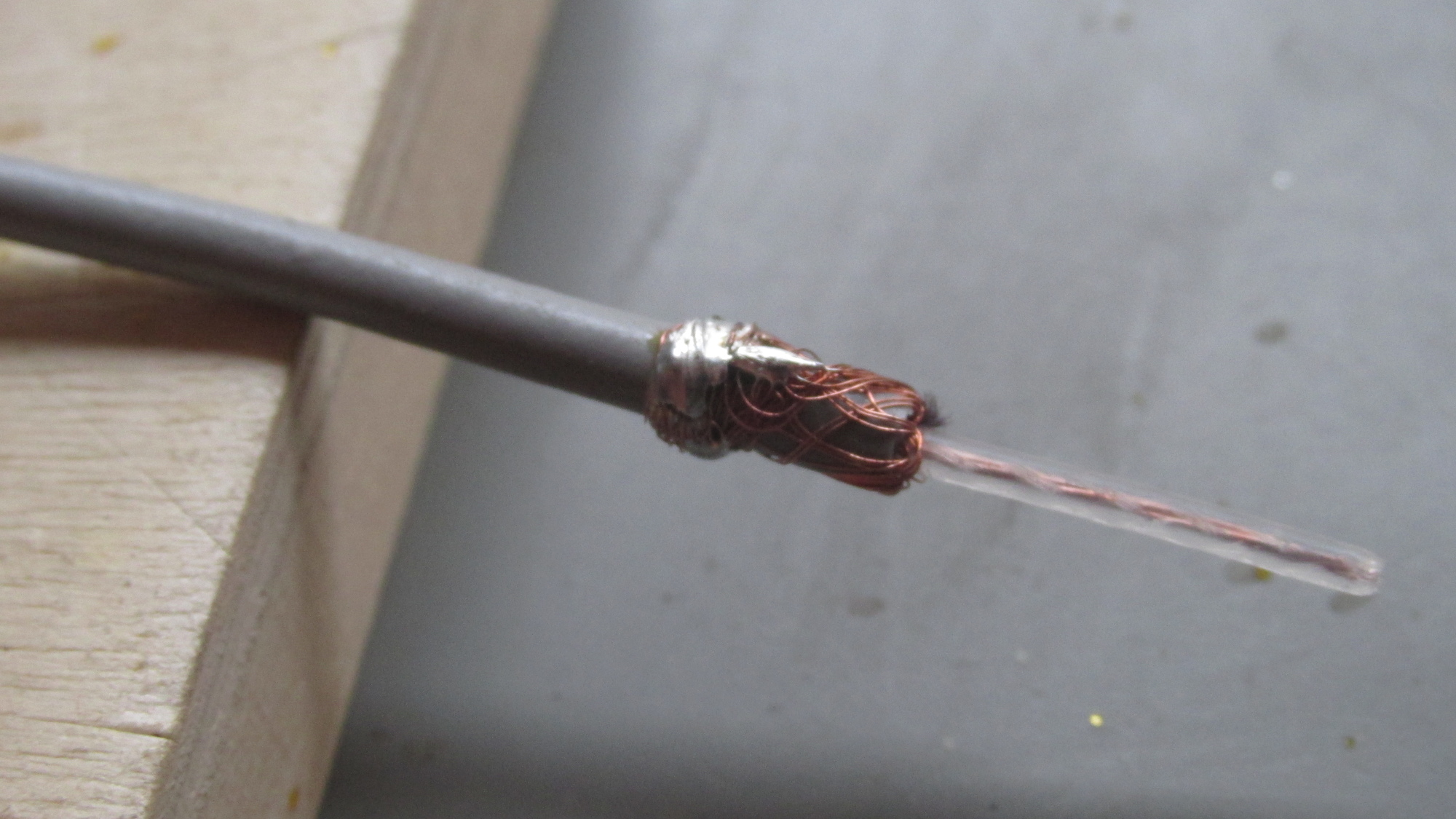
Seal shield with solder.
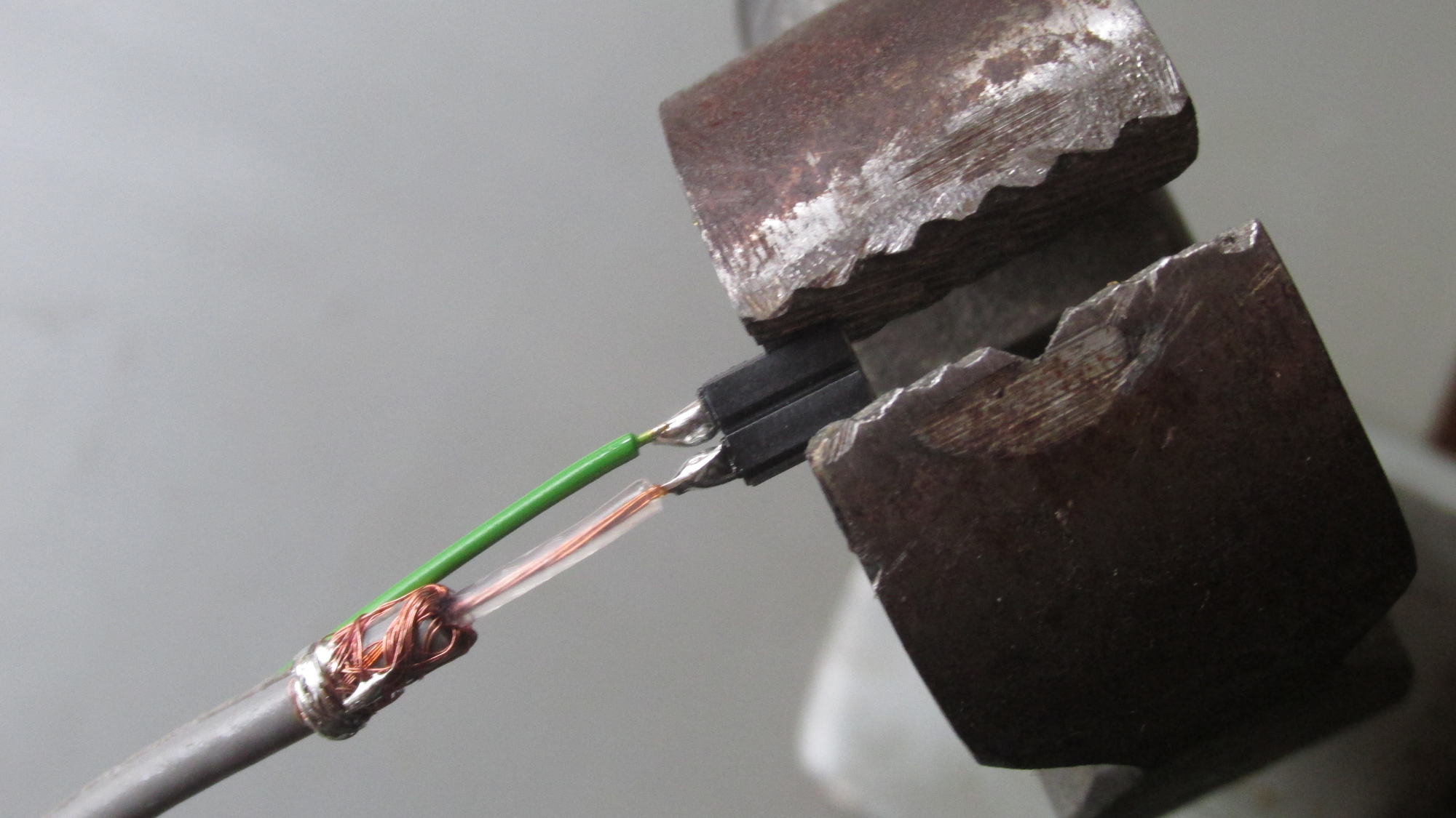
Pair clock wire with green cable, neighbouring the yellow wire.
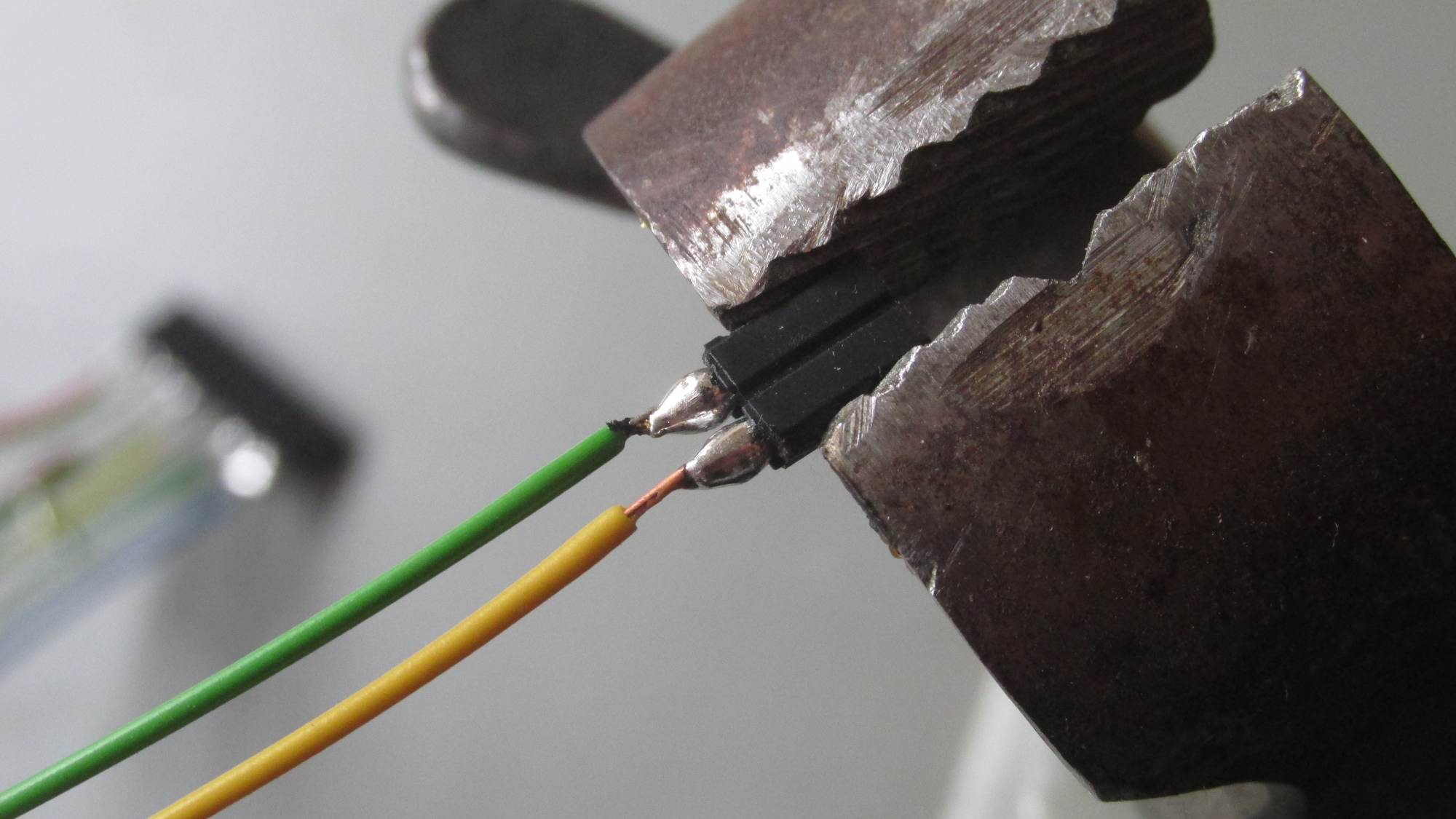
Pair colored wires with their neighbouring green wires.
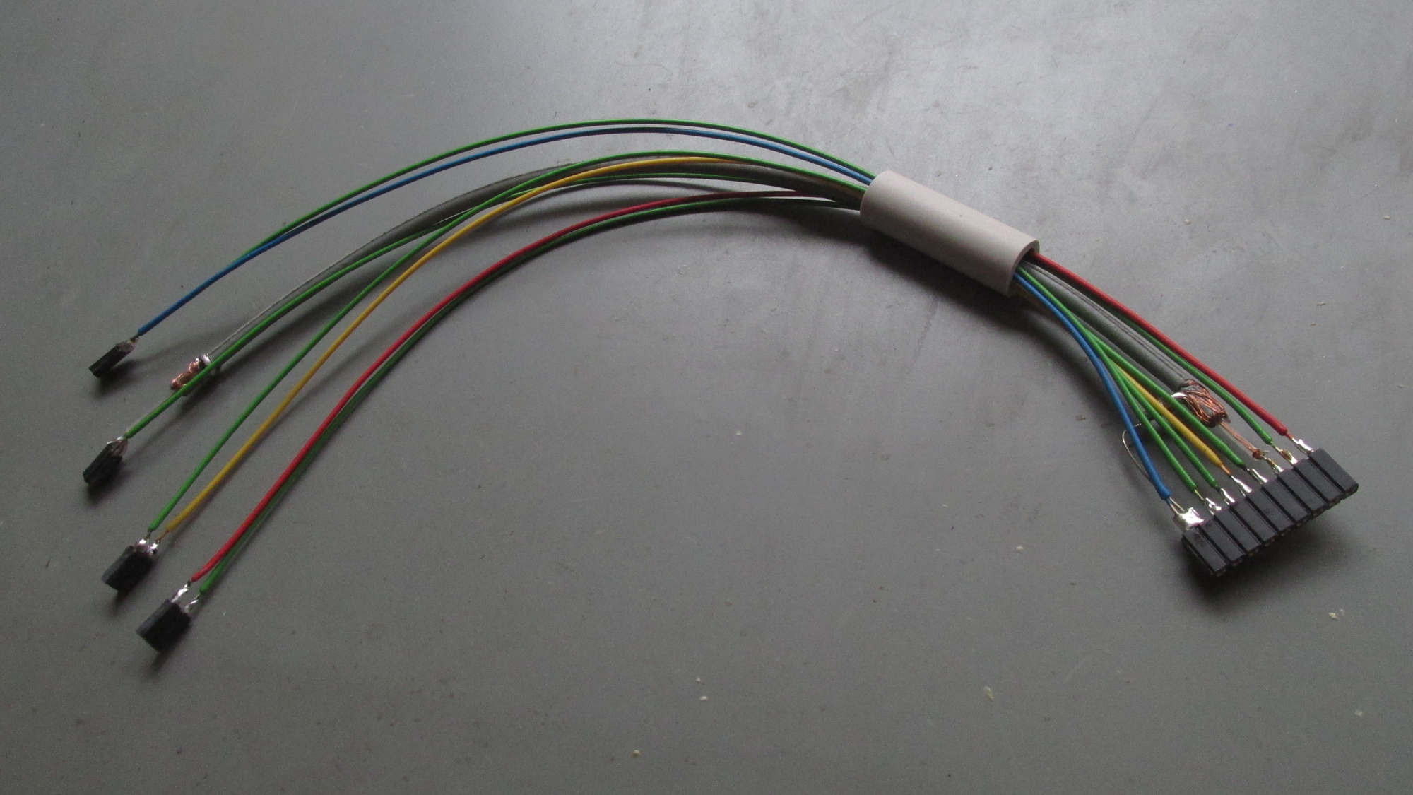
Done.
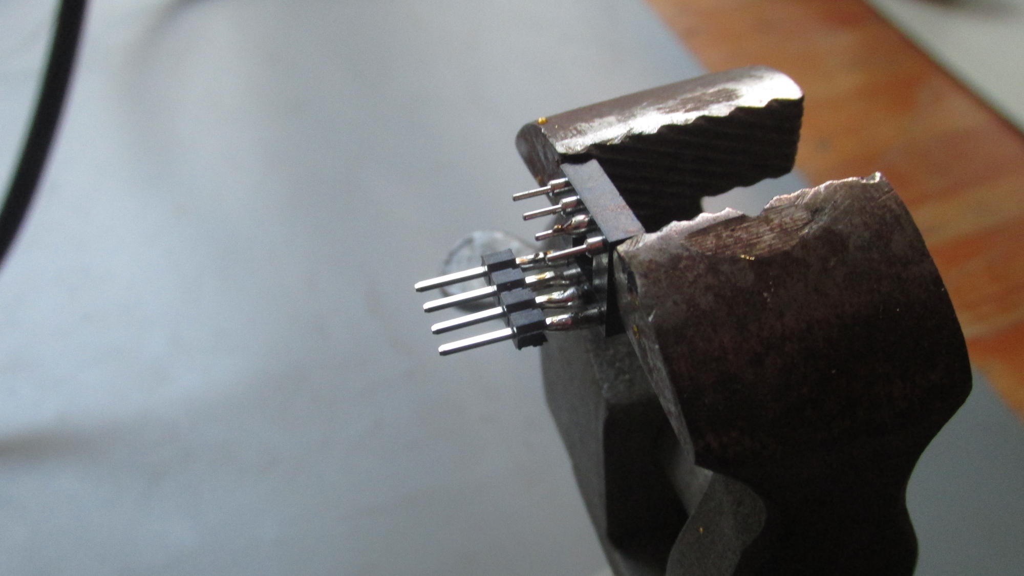
Add two 4×1 pinheader to DIL8 Socket.
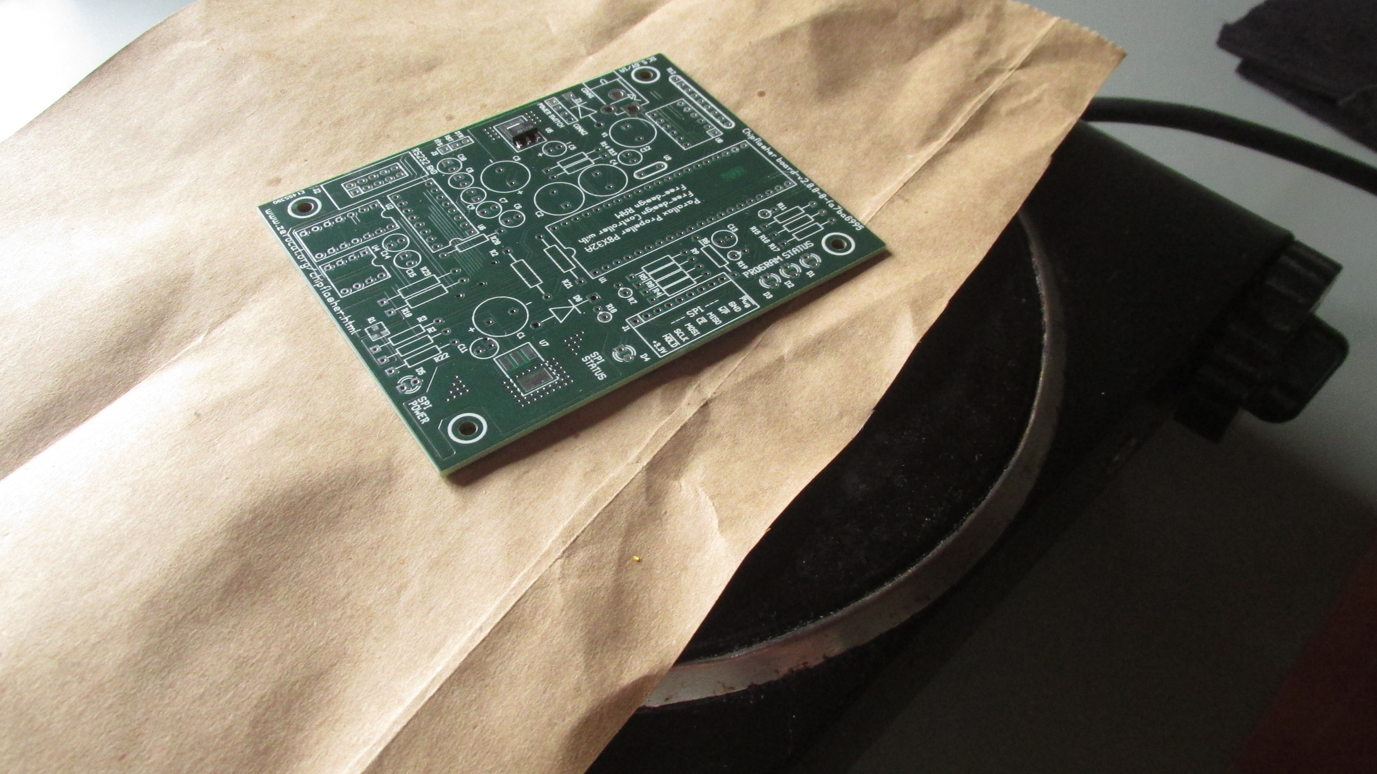
U5: Preheat on Cooking Plate
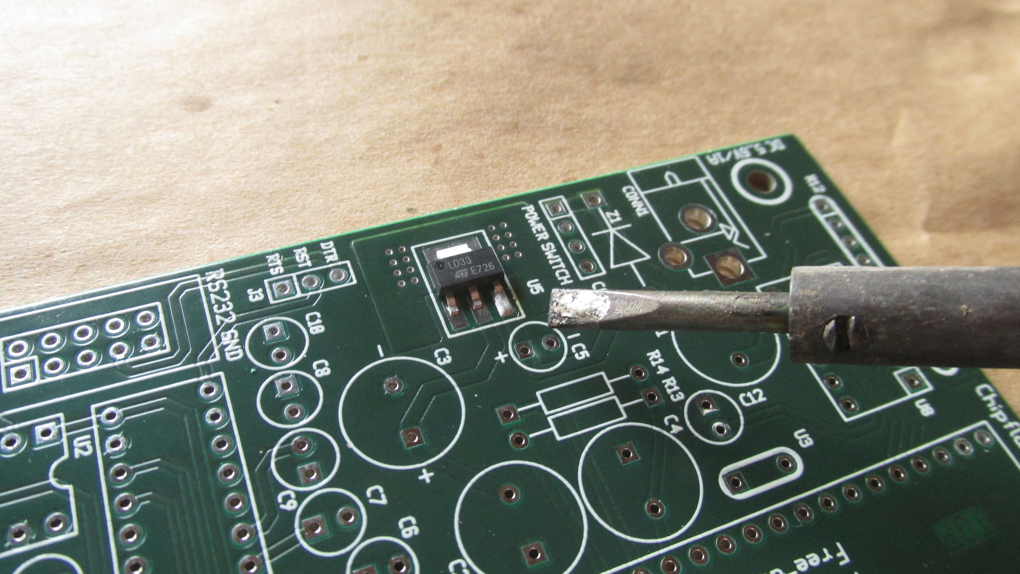
U5: Fix position using one pin
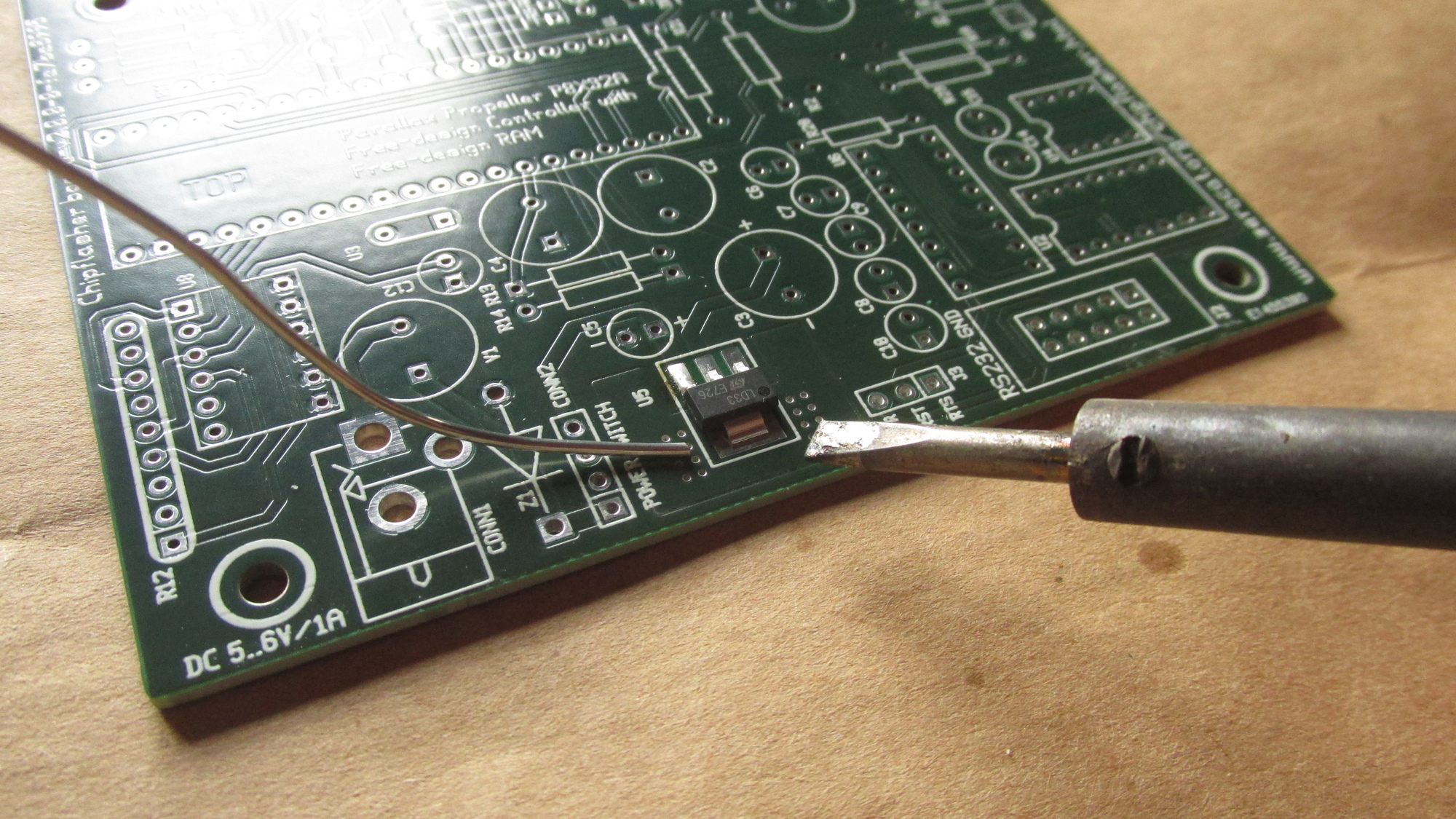
U5: Turn plate on for 5 seconds, solder tab using 1mm solder.
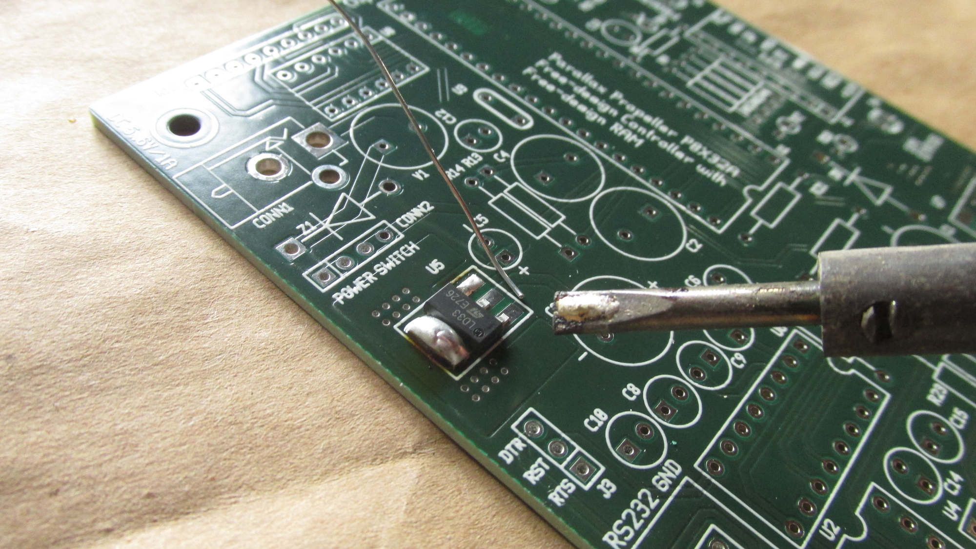
U5: Solder pins using 0.5mm solder
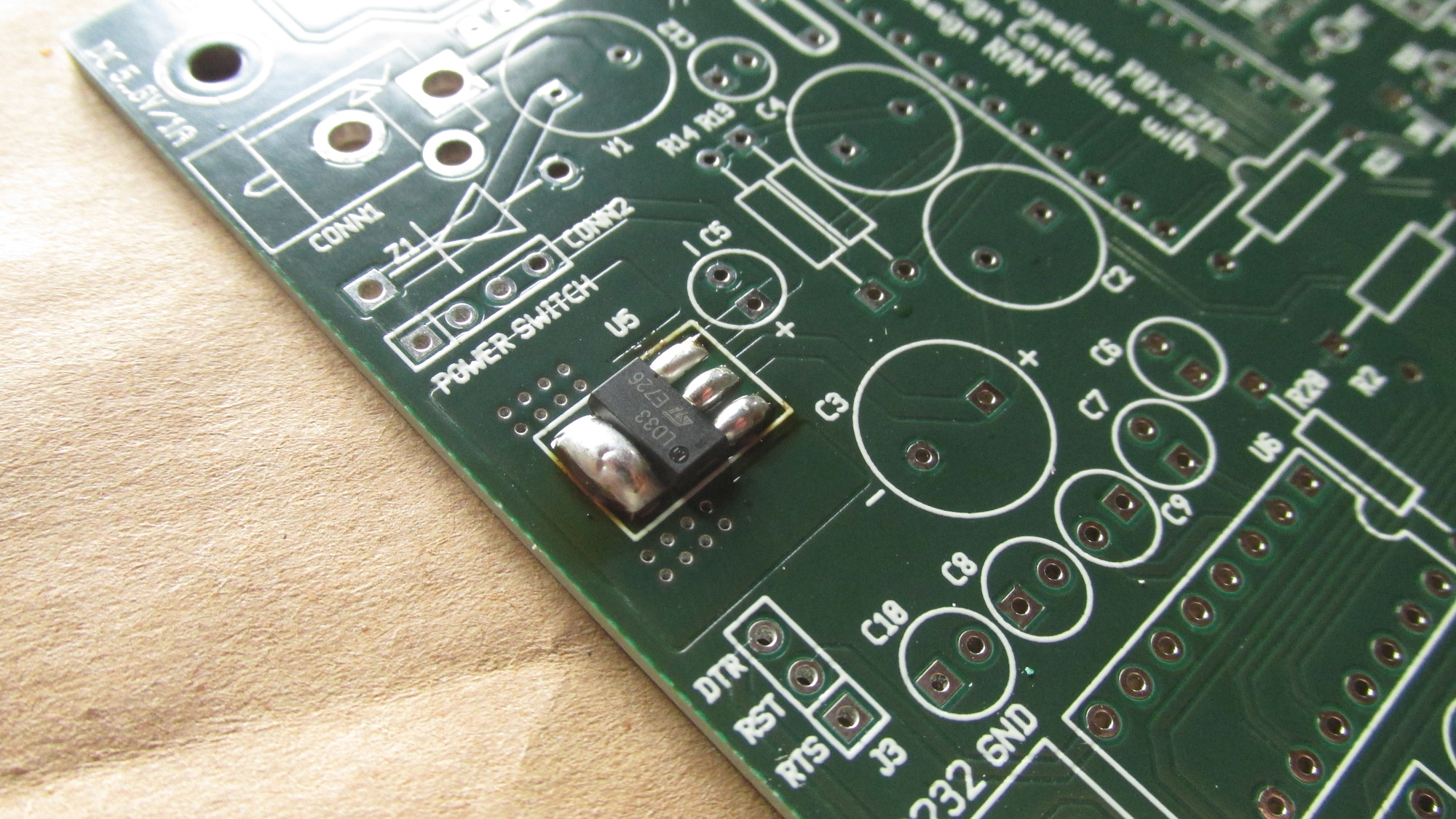
U5: Done.
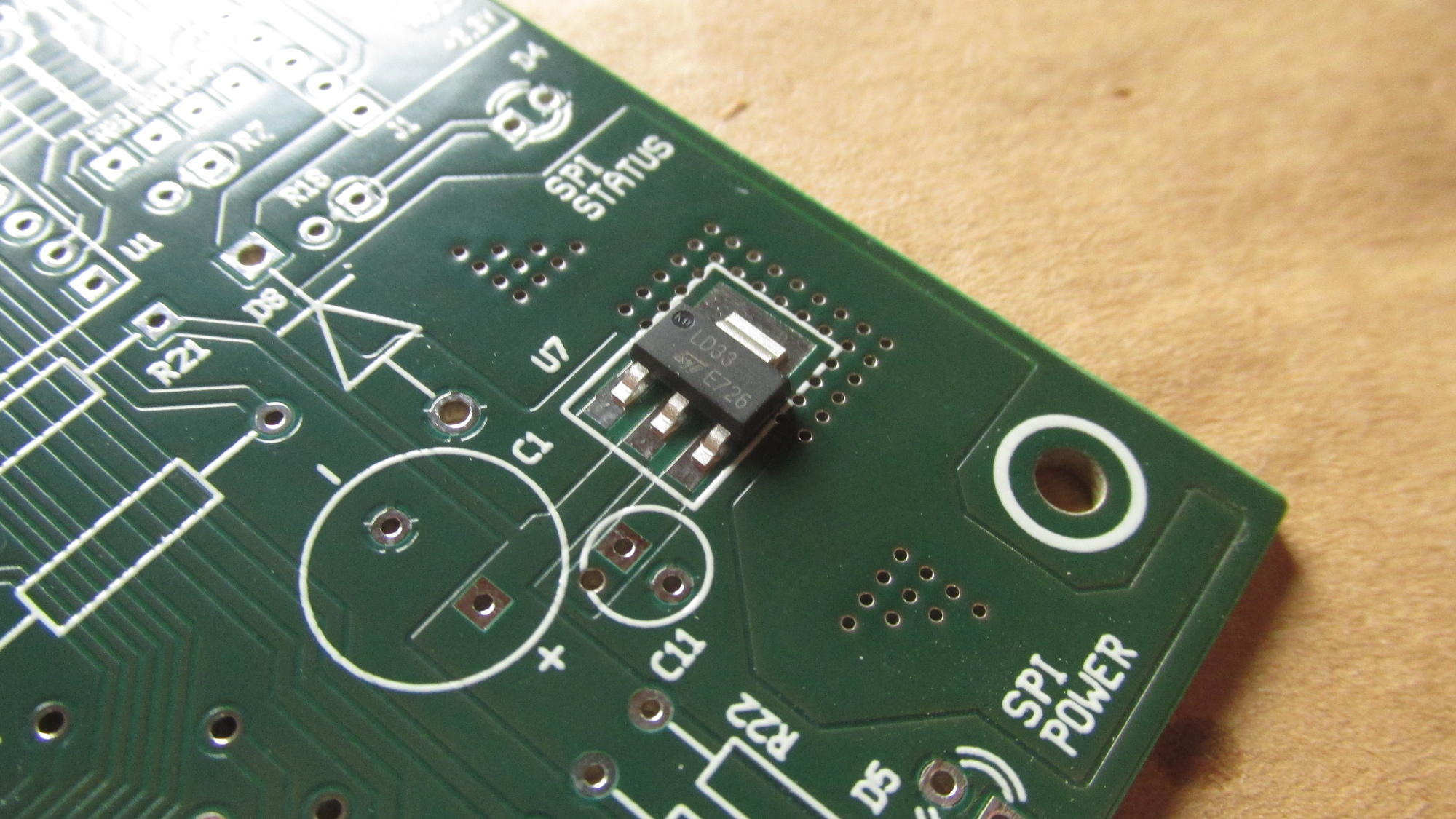
U7: Place U7, still on Cooking Plate
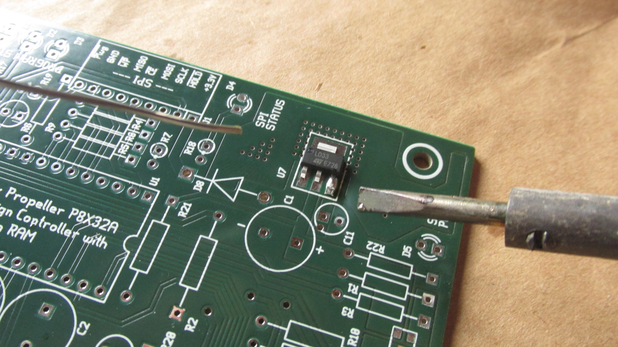
U7: Fix position using on pin
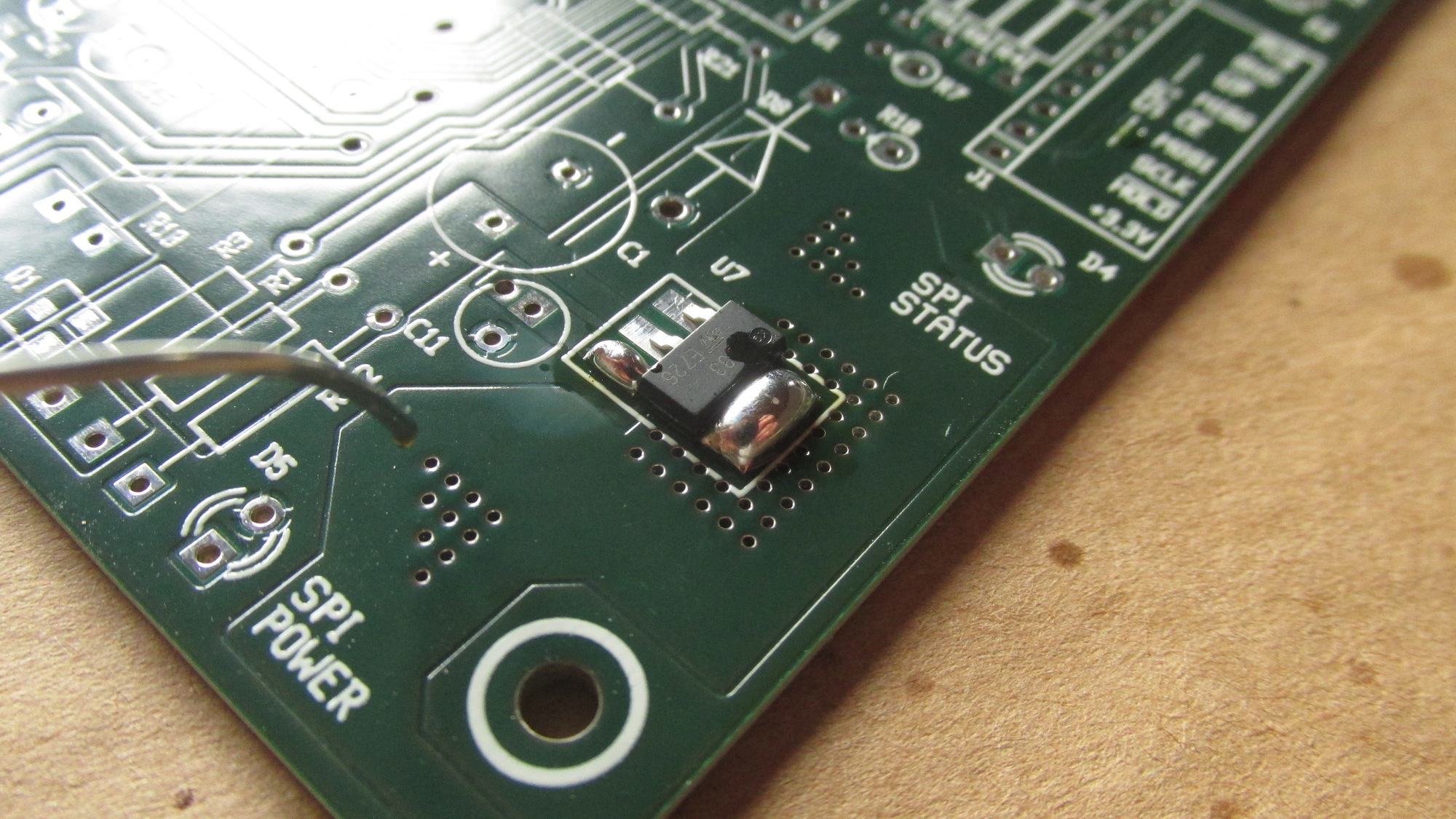
U7: Turn Plate on for another 5 seconds, solder tab using 1mm solder
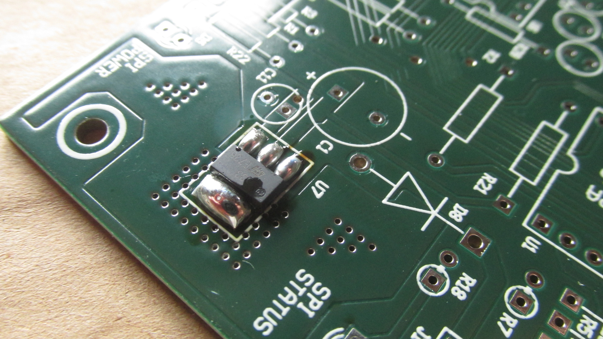
U7: Solder other pins using 0.5mm solder, done
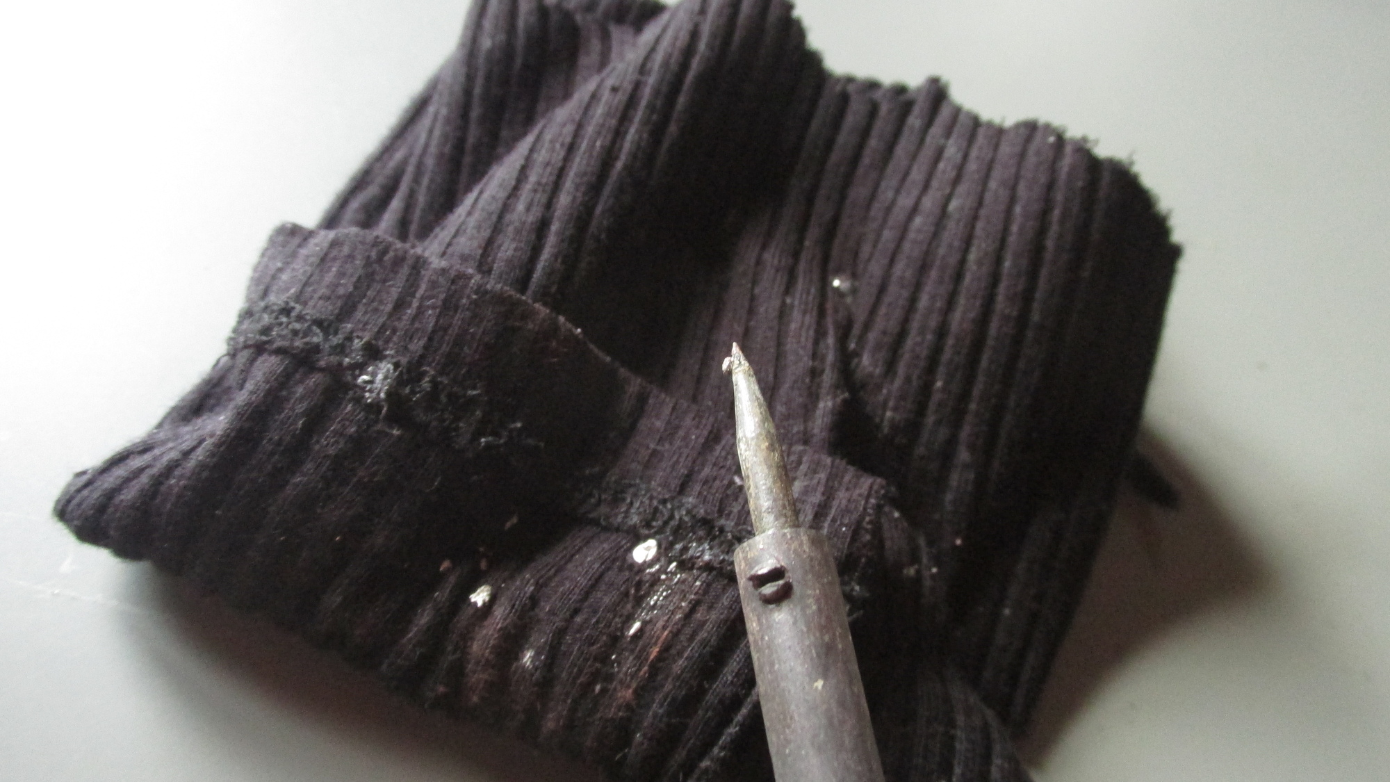
Change solder tip, clean tip on wet cloth
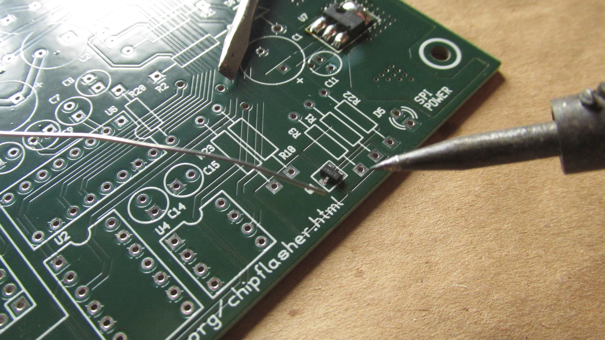
Q1: Place MOSFET, put screwdriver nearby, preheat PCB for 3 to 5 seconds
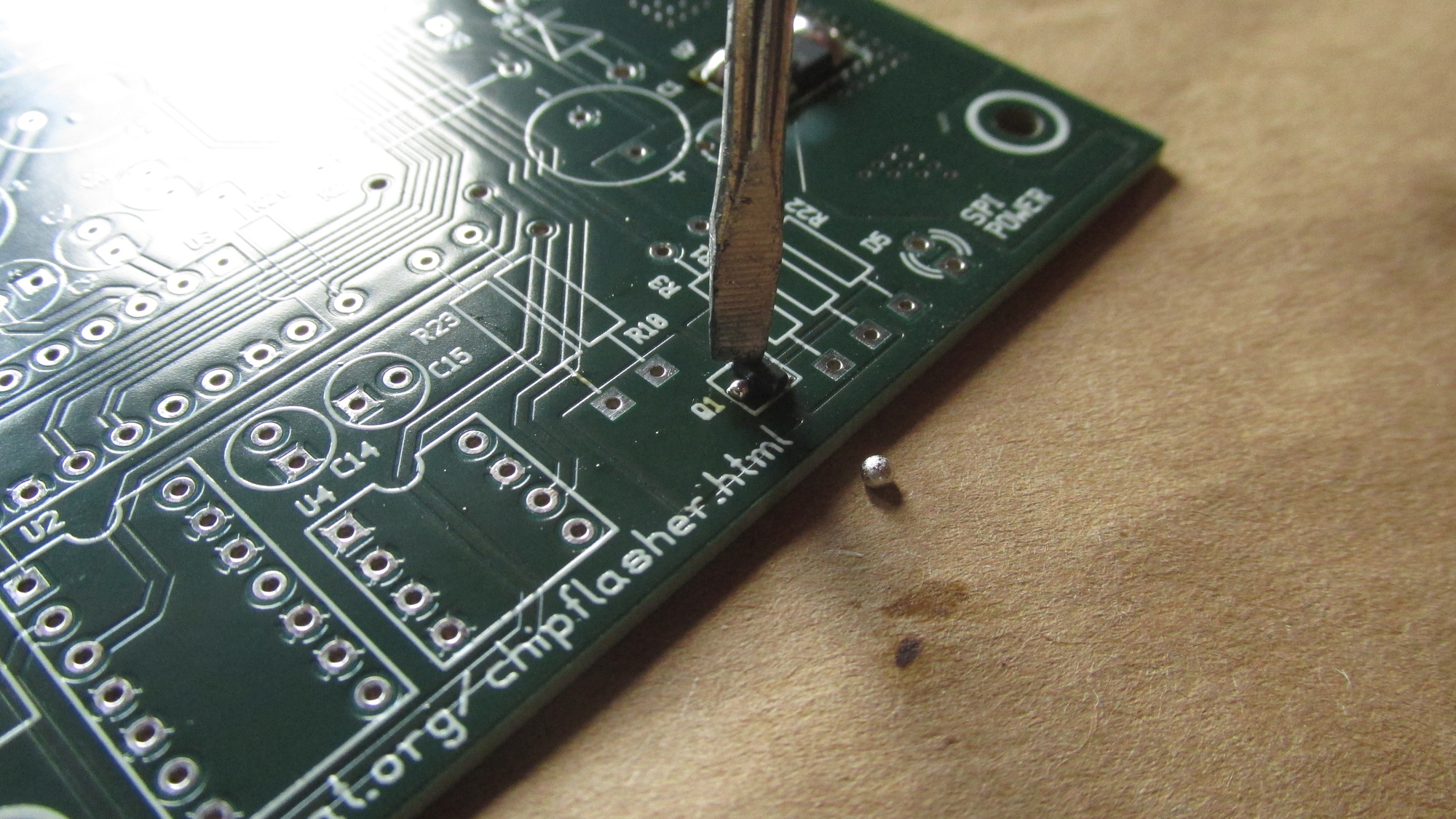
Q1: Add solder to tip, fix Q1 with screwdriver and solder first pad
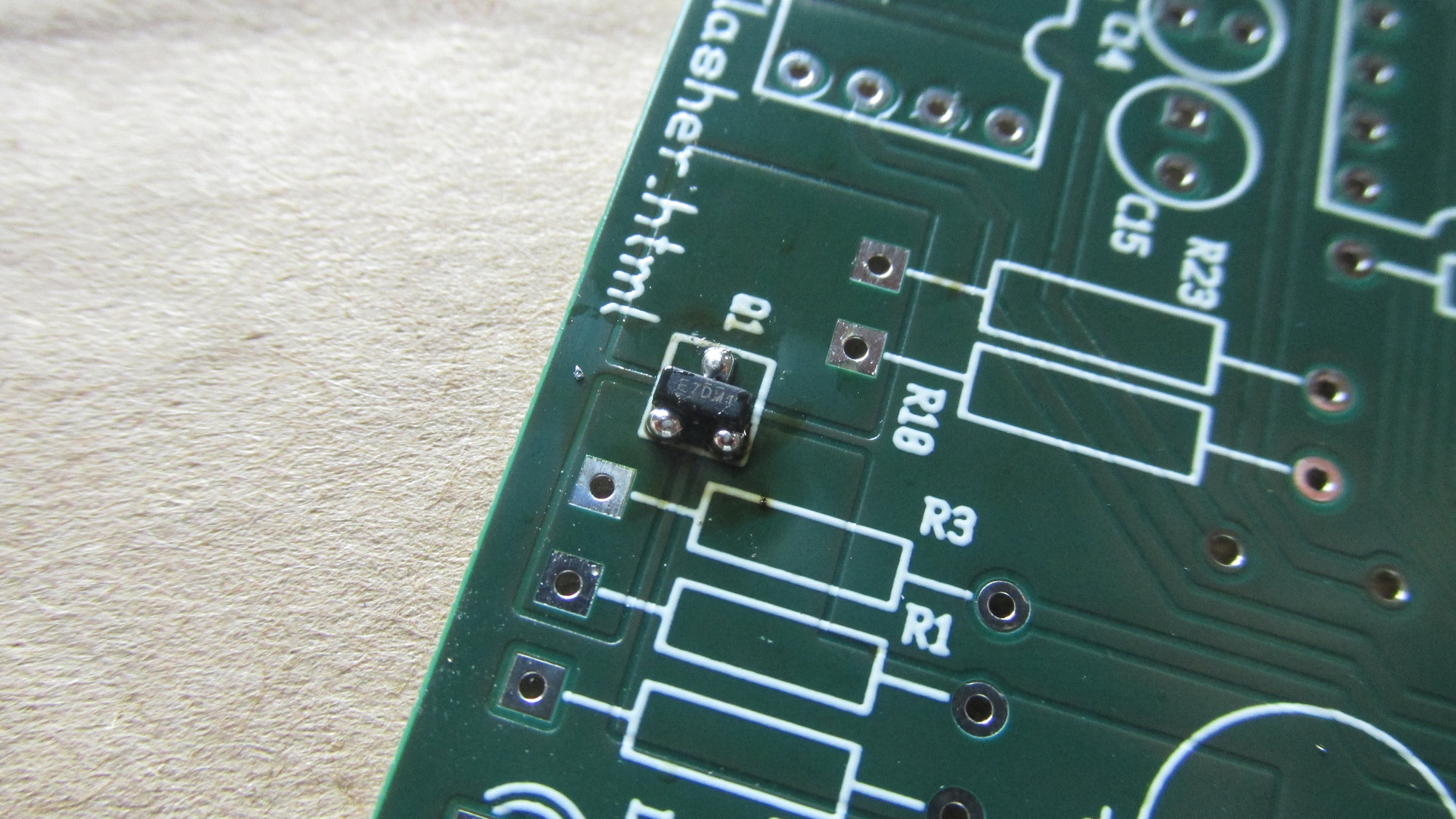
Q1: Solder other pads, make sure pins of R3 and R10 are not polluted
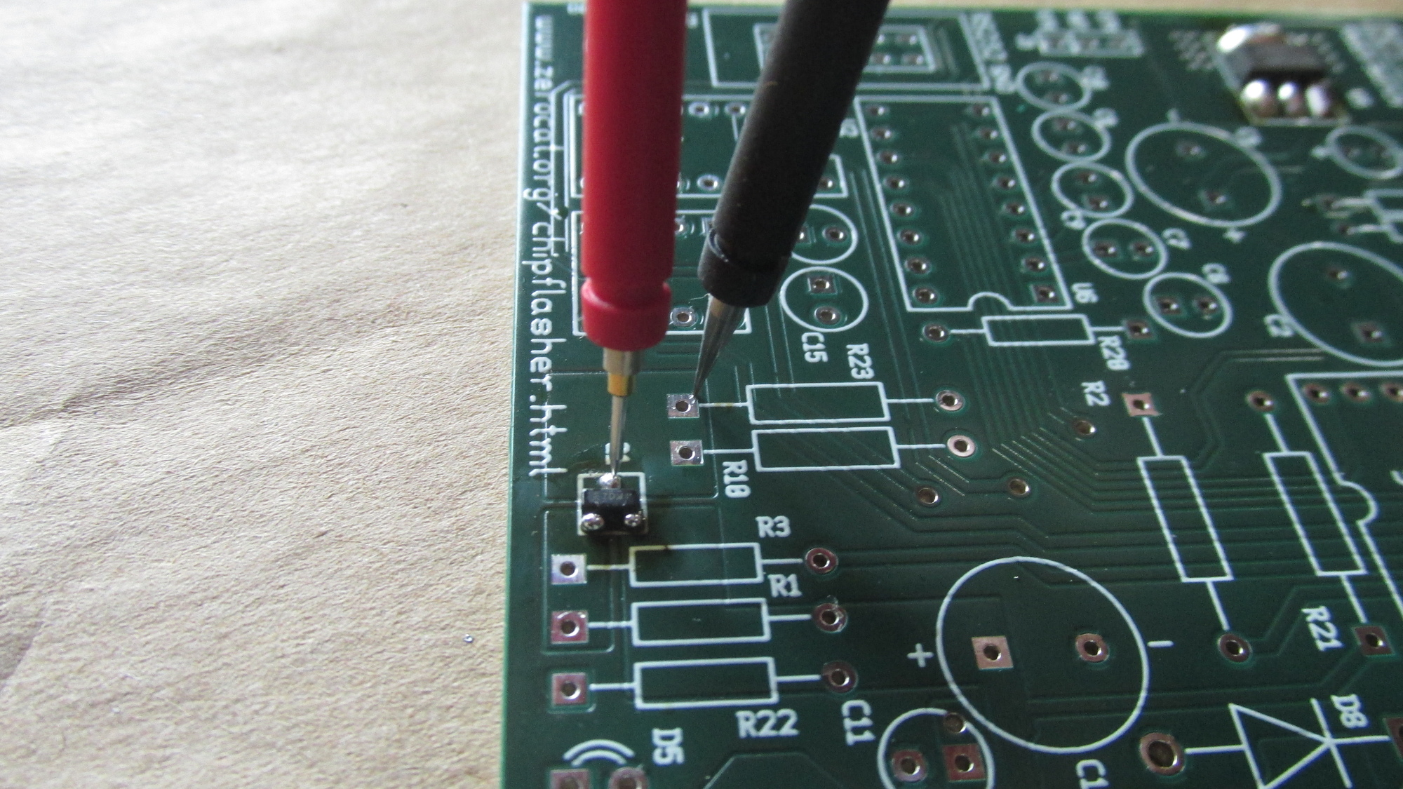
Q1: Check electrical connection with probe, done
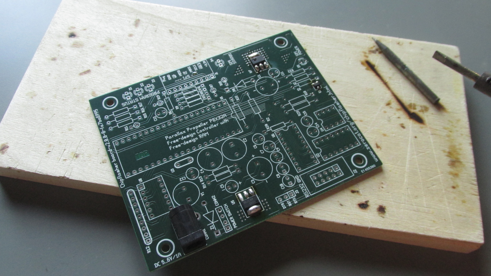
CONN1: Move PCB onto breadboard, place part, change solder tip (careful, it’s hot!)
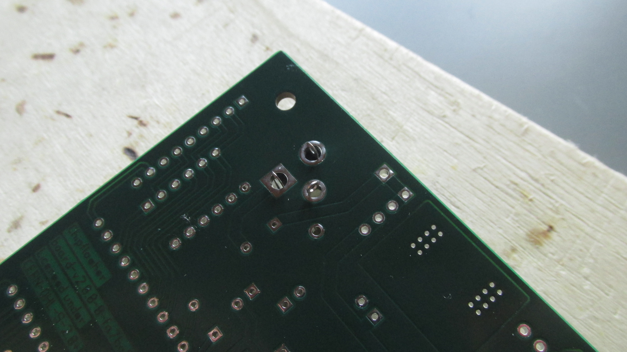
CONN1: Flip PCB, locate pins
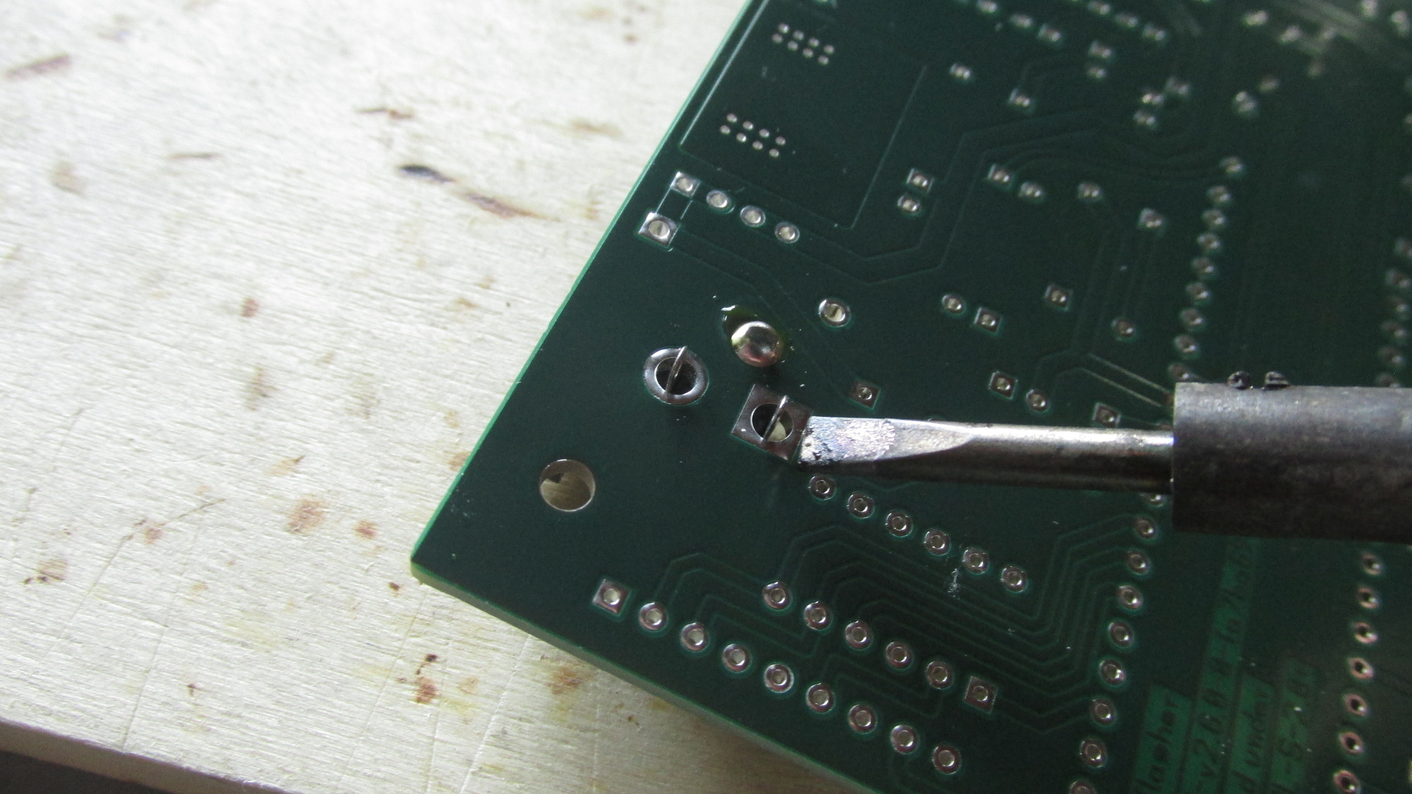
CONN1: Solder pins using 1mm solder, first heat pads, then heat pins! Be quick!
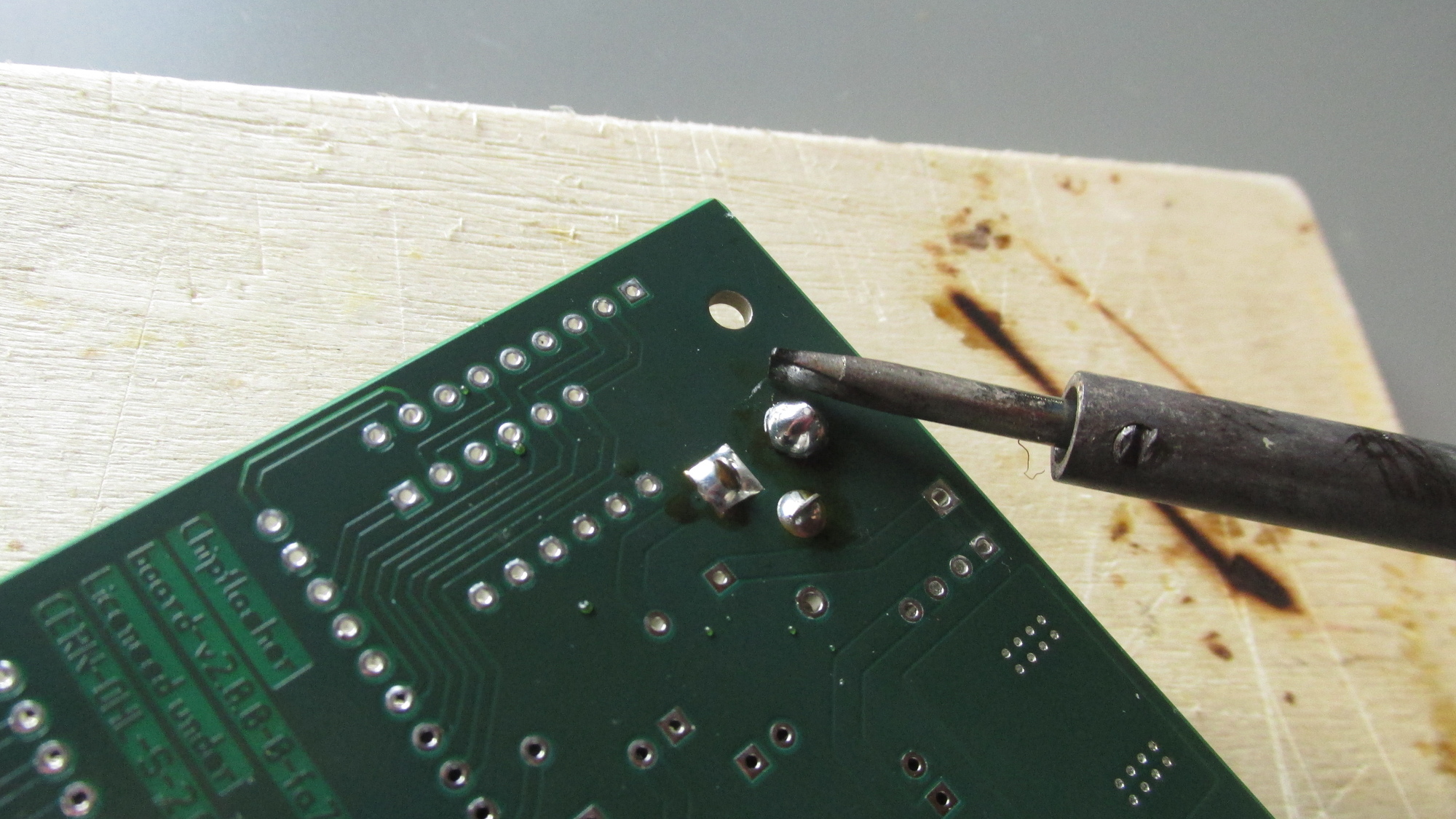
CONN1: Solder GND pin, use full surface of solder tip to apply heat as fast as possible!
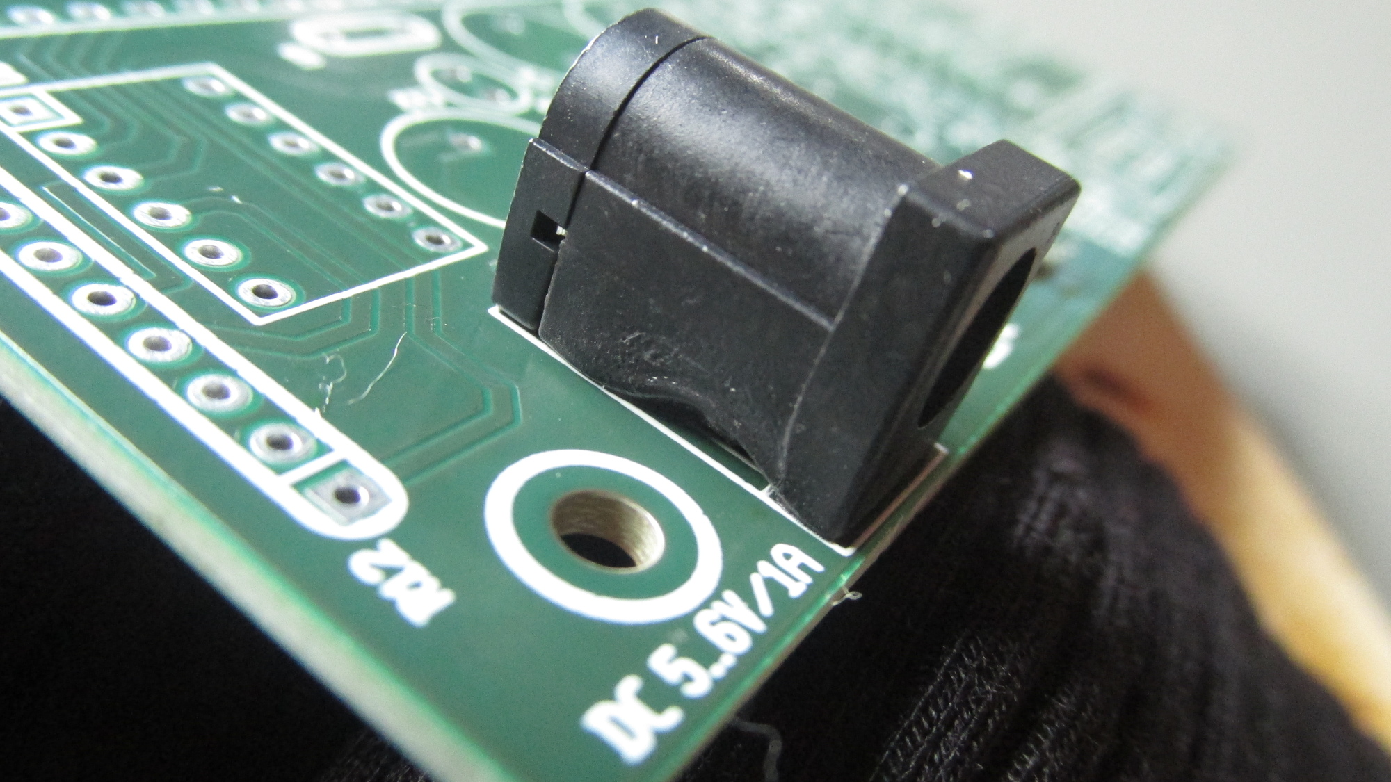
CONN1: Uooh, part became too hot, it is melted. How to apply heat in a faster way??
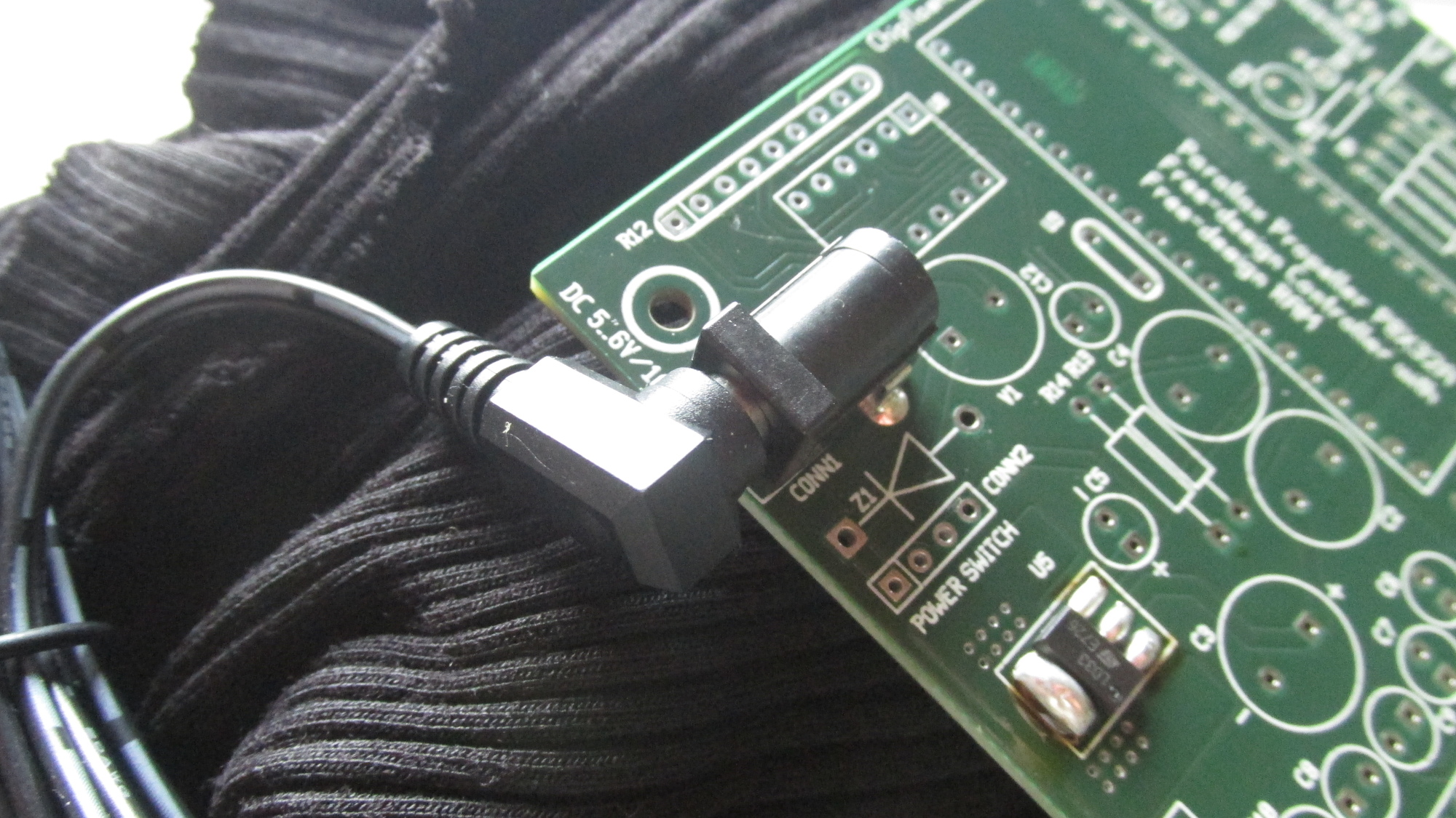
CONN1: Check mechanical functionality
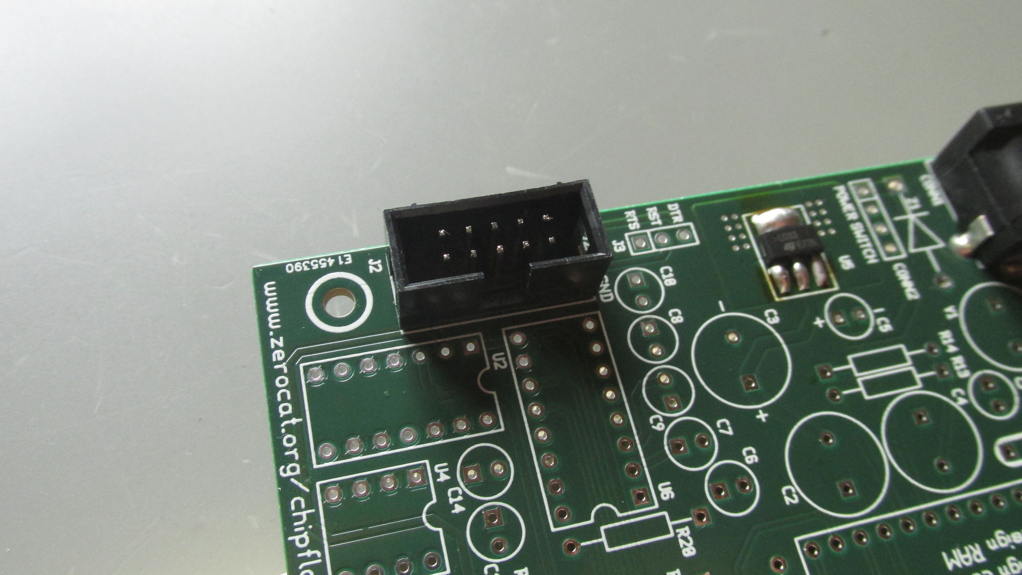
J2: Place part
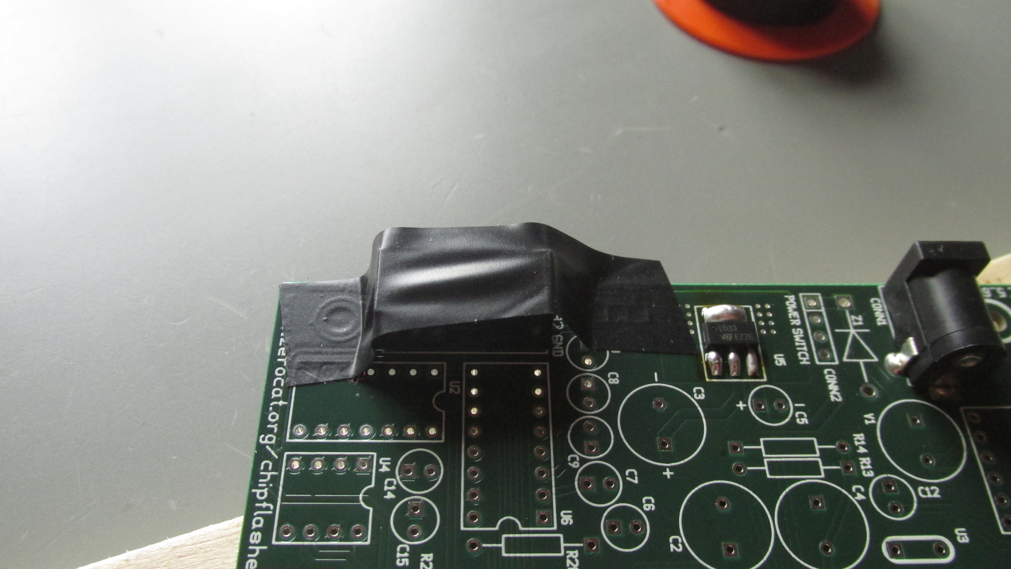
J2: Fix on PCB with tape
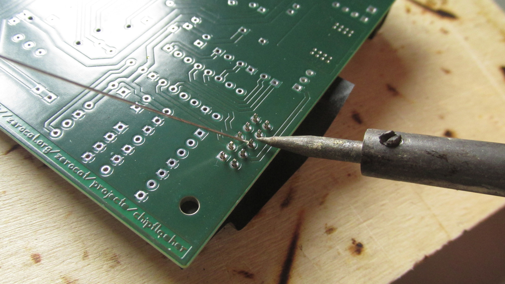
J2: Solder one center pin
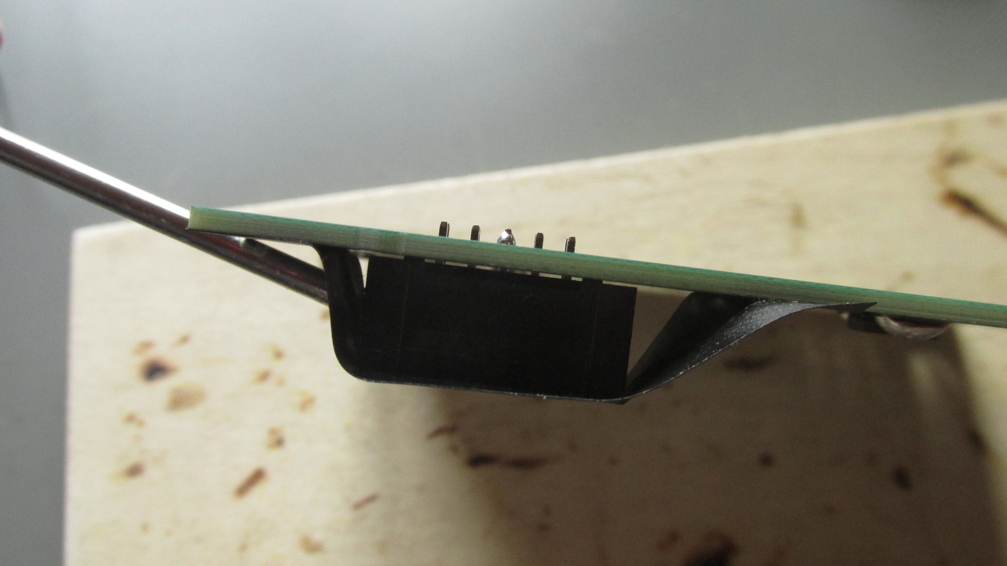
J2: Check proper, flat position on PCB
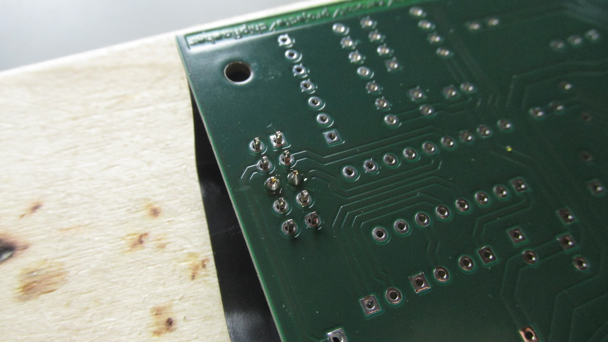
J2: Solder next center pin
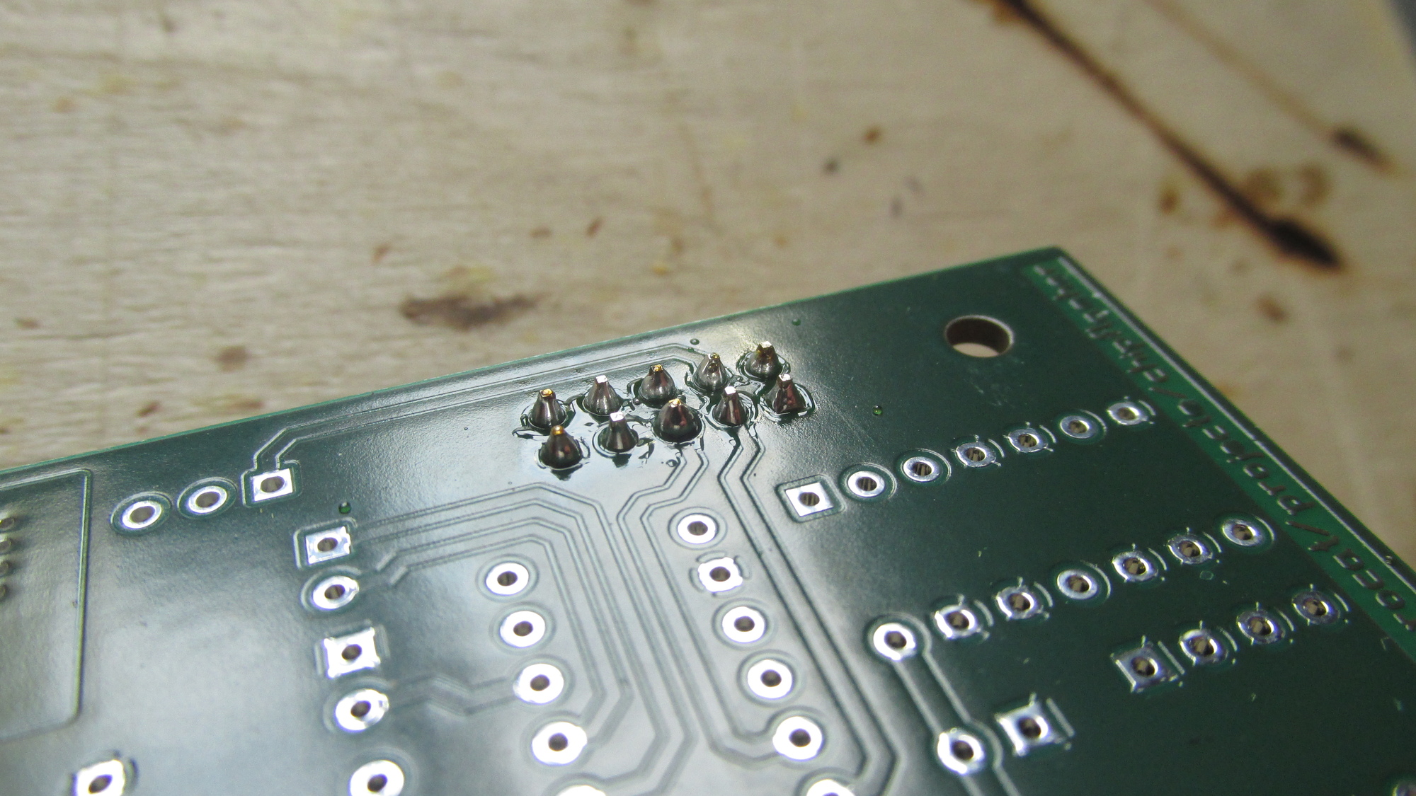
J2: Solder remaining pins, GND pin set as thermal will heat up like 3 times slower
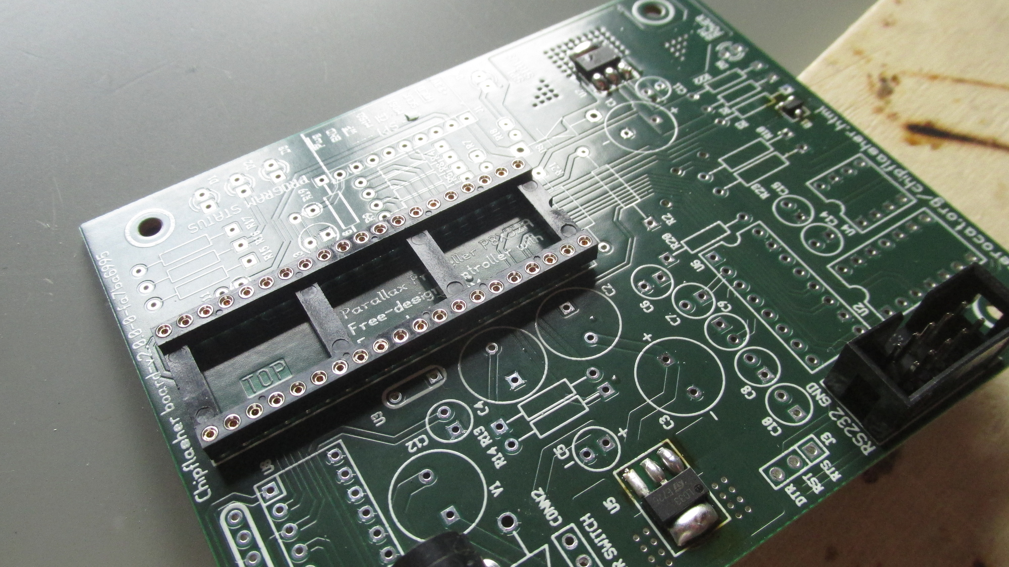
U1 Socket: Place socket on PCB
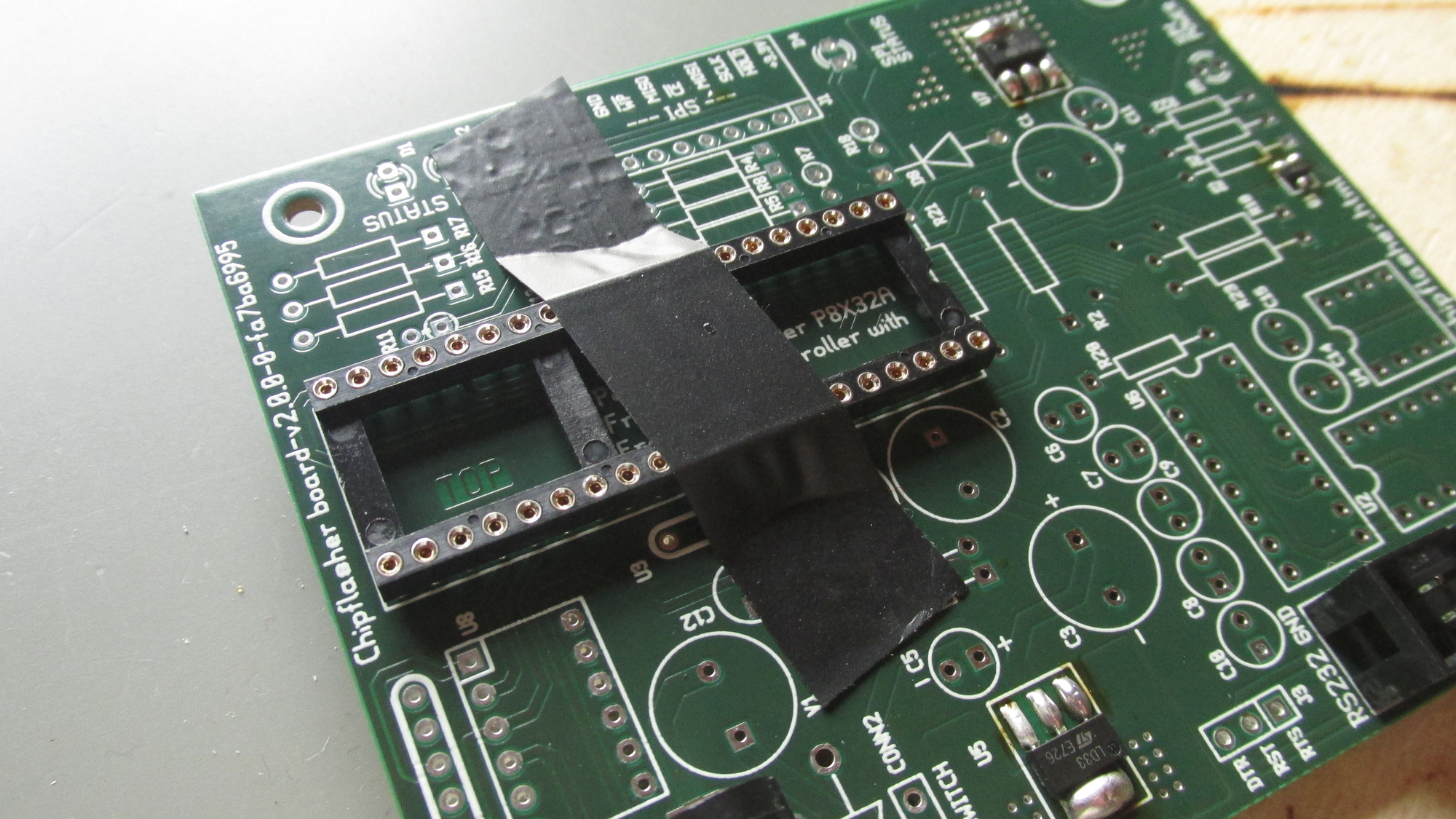
U1 Socket: Fix with tape
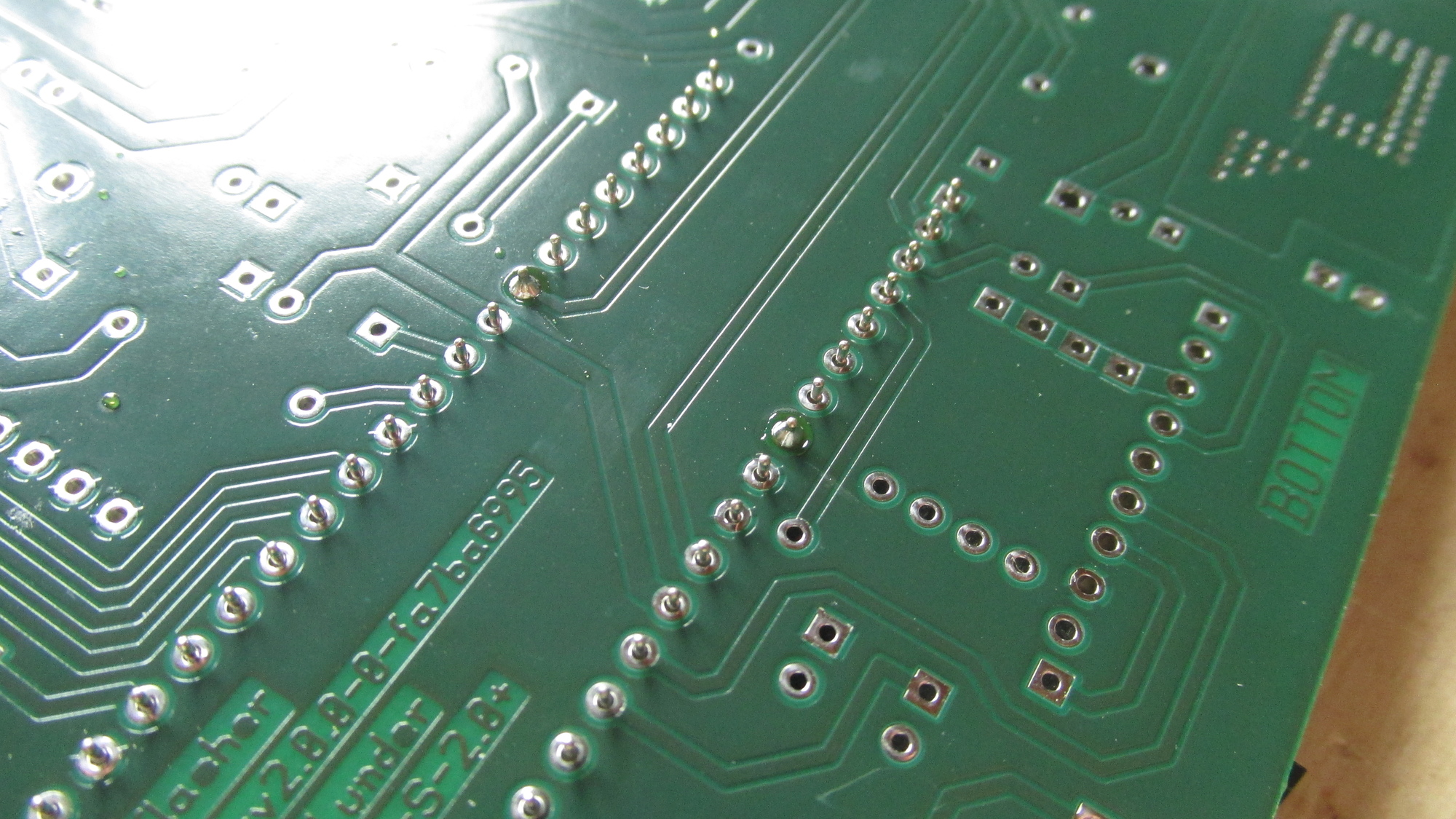
U1 Socket: Solder center pins, do not start with thermals!
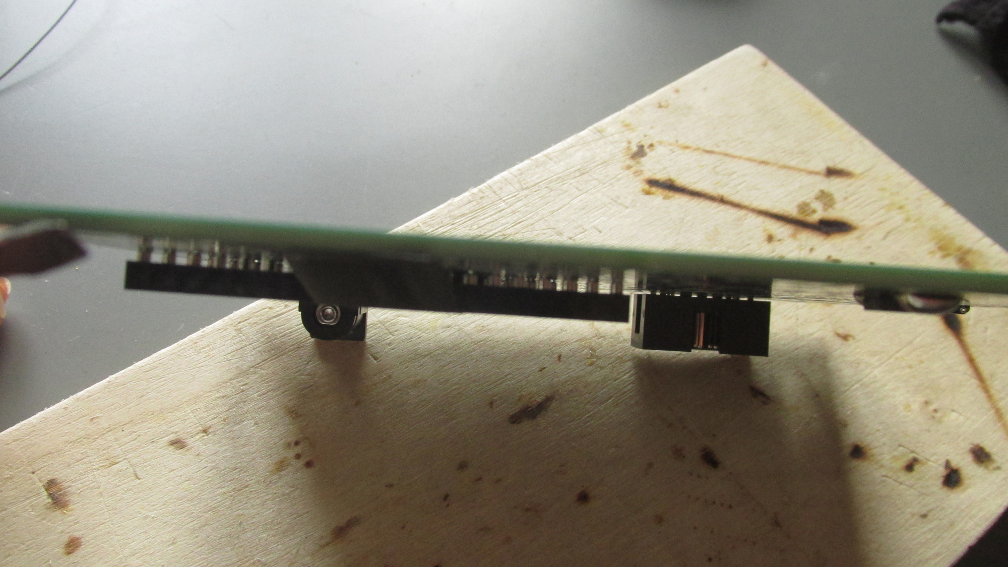
U1 Socket: Check for flat socket position on PCB
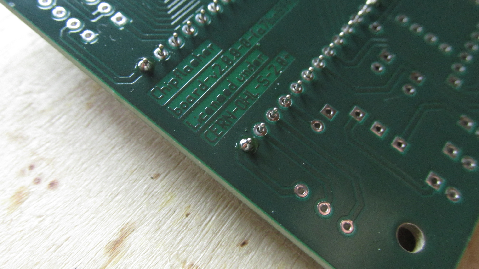
U1 Socket: Solder pairs of first and last pins, check for flat position again
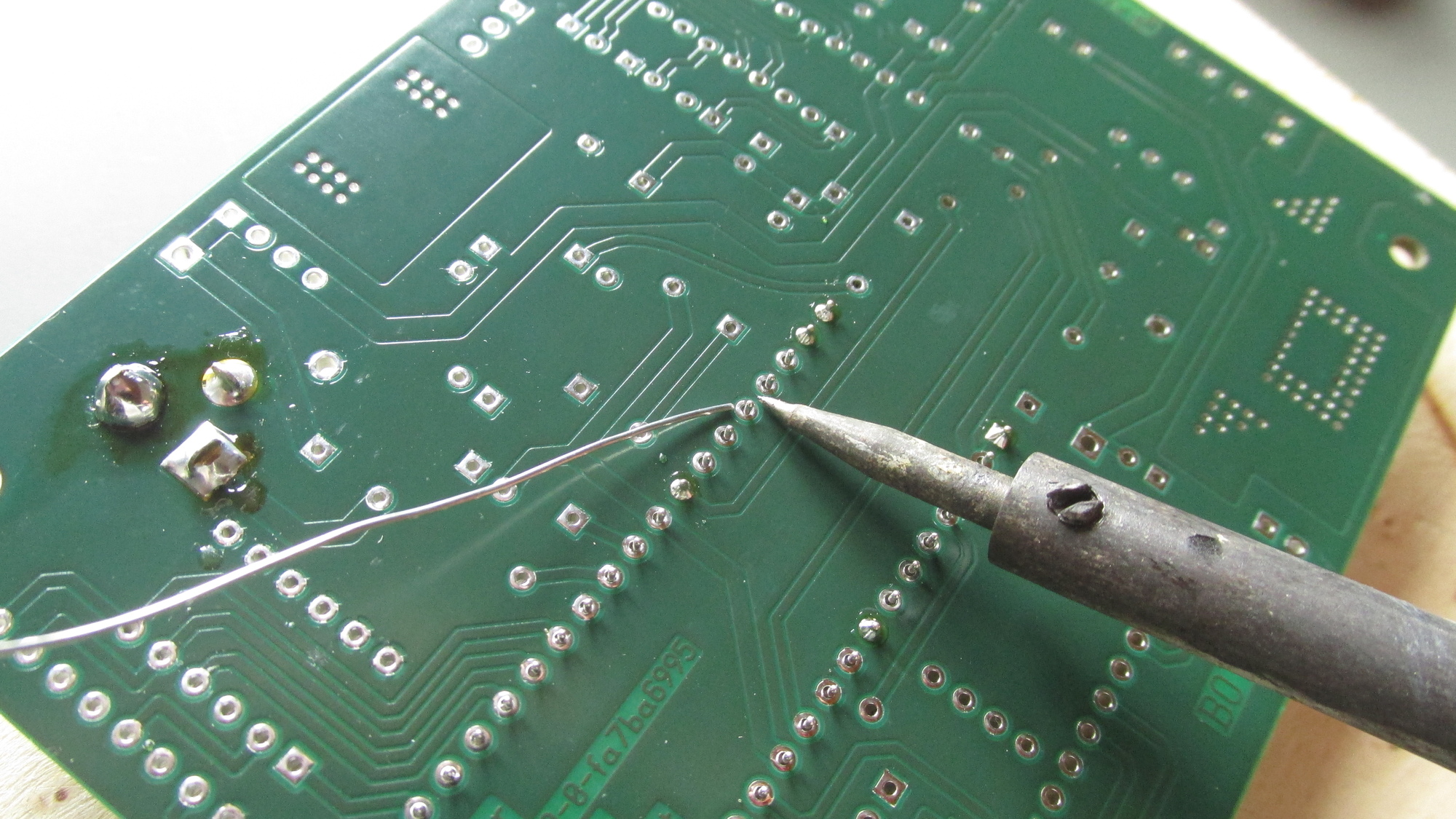
U1 Socket: Solder remaining pins, thermals will heat up like 3 to 5 times slower!
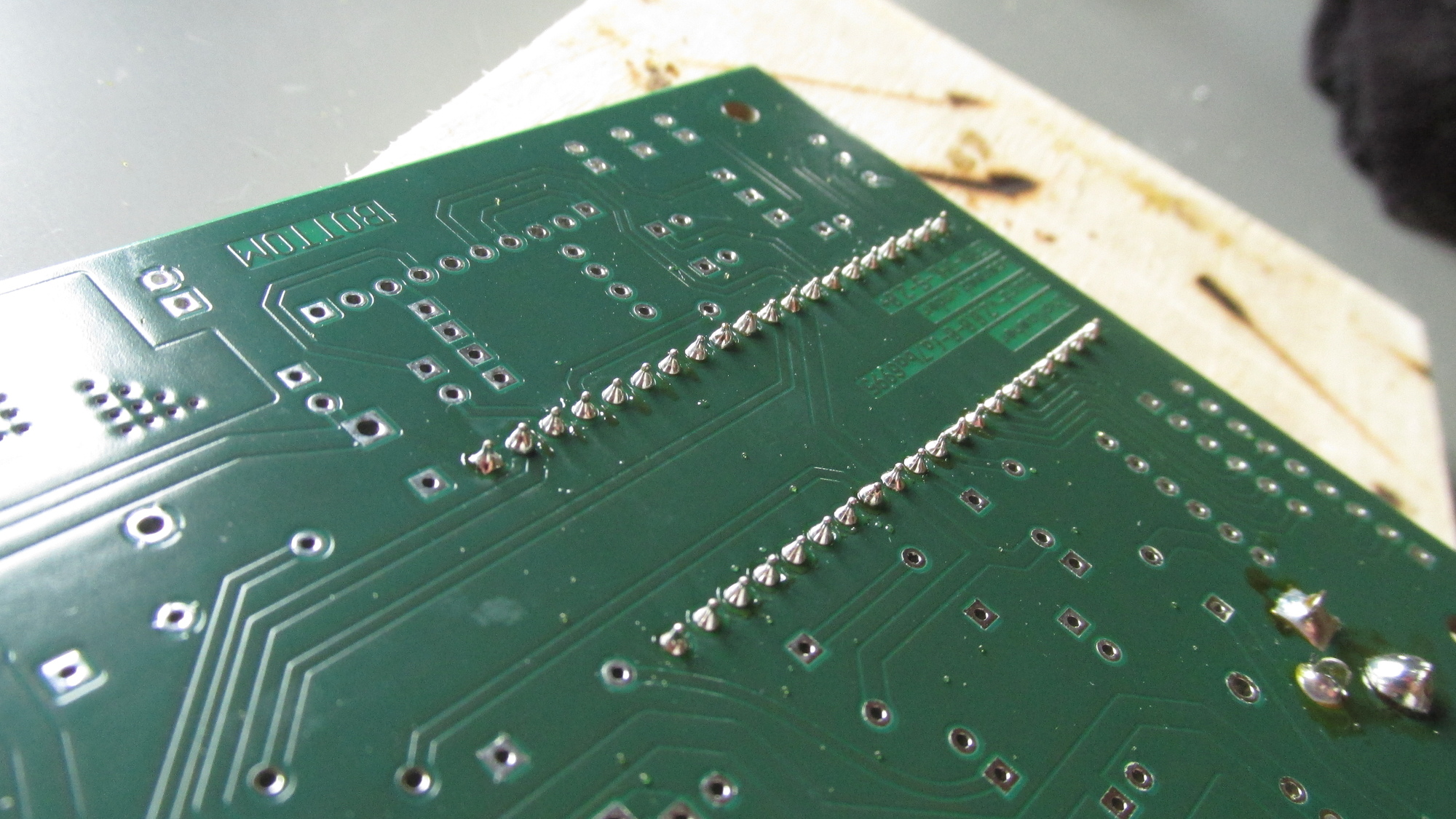
U1 Socket: Done
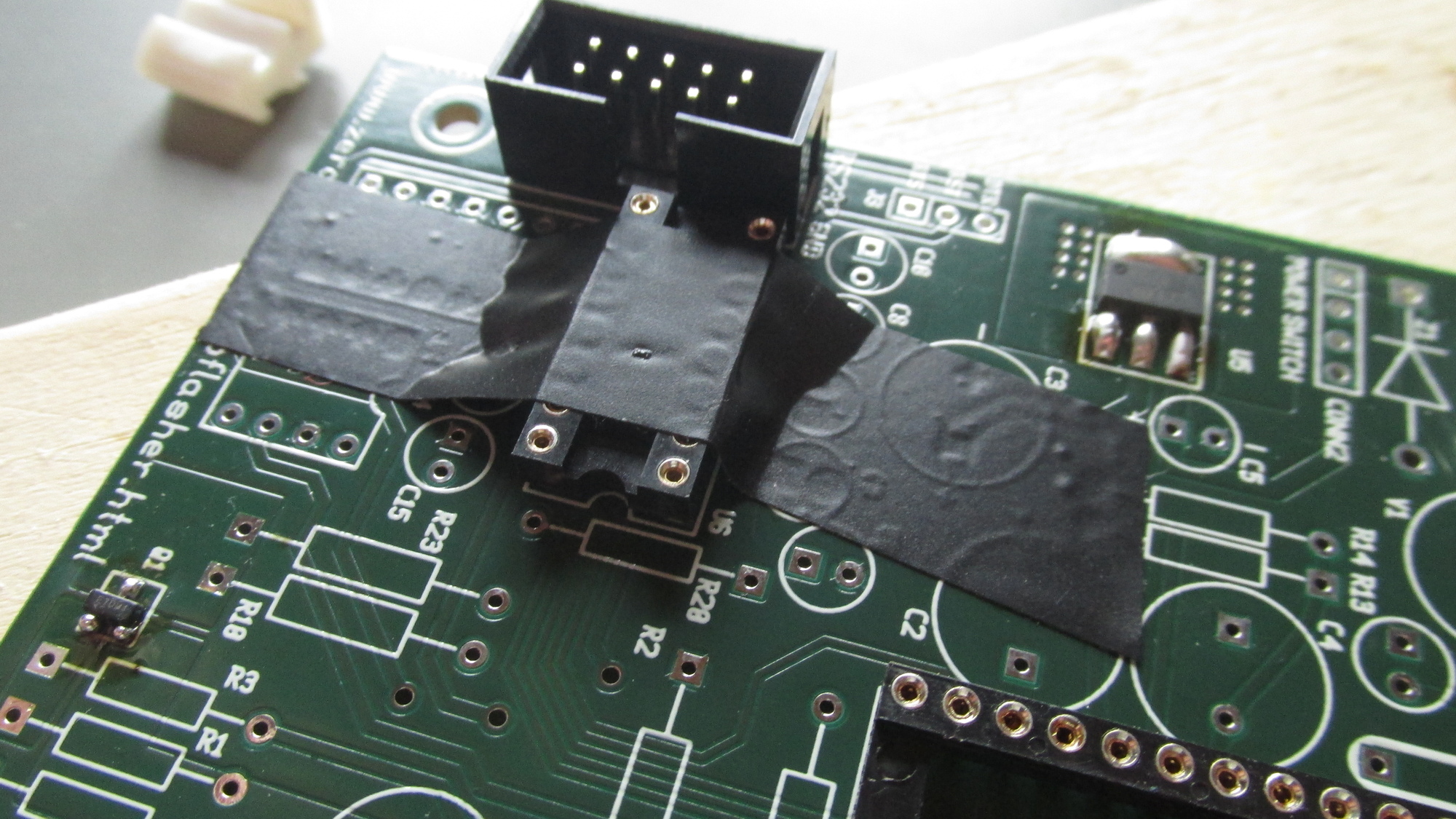
U6 Socket: Place on PCB, fix with tape
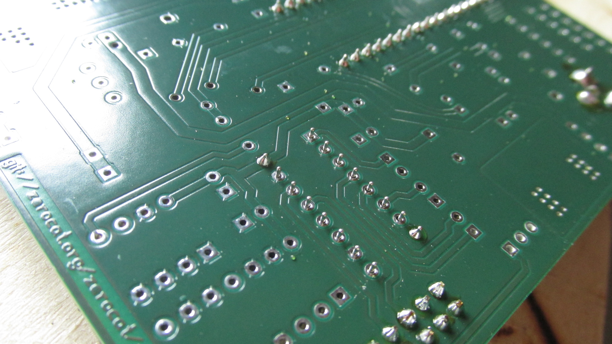
U6 Socket: Solder two diagonal edge pins, check for flat socket position
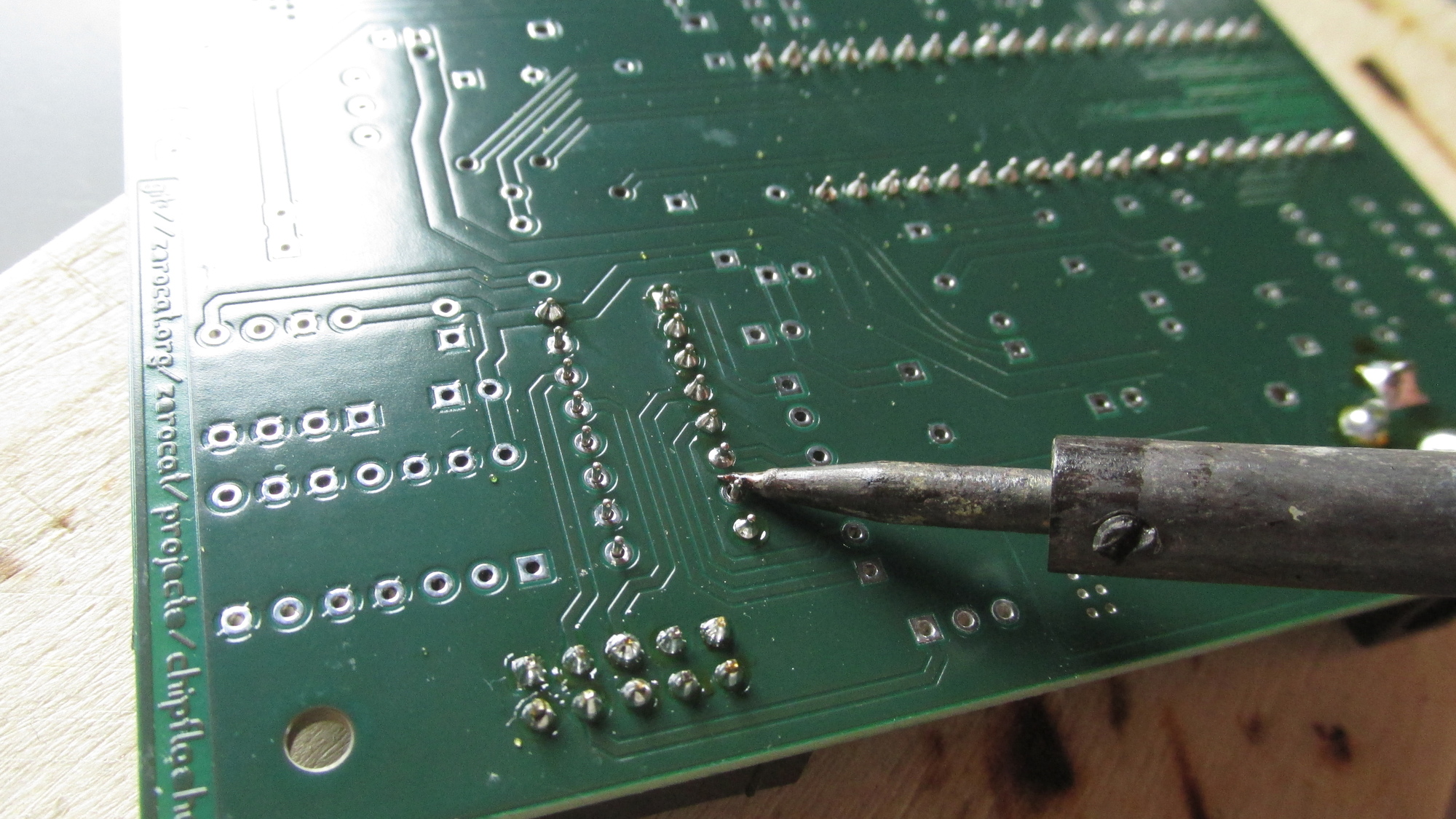
U6 Socket: Solder remaining pins, thermals will heat up slower!
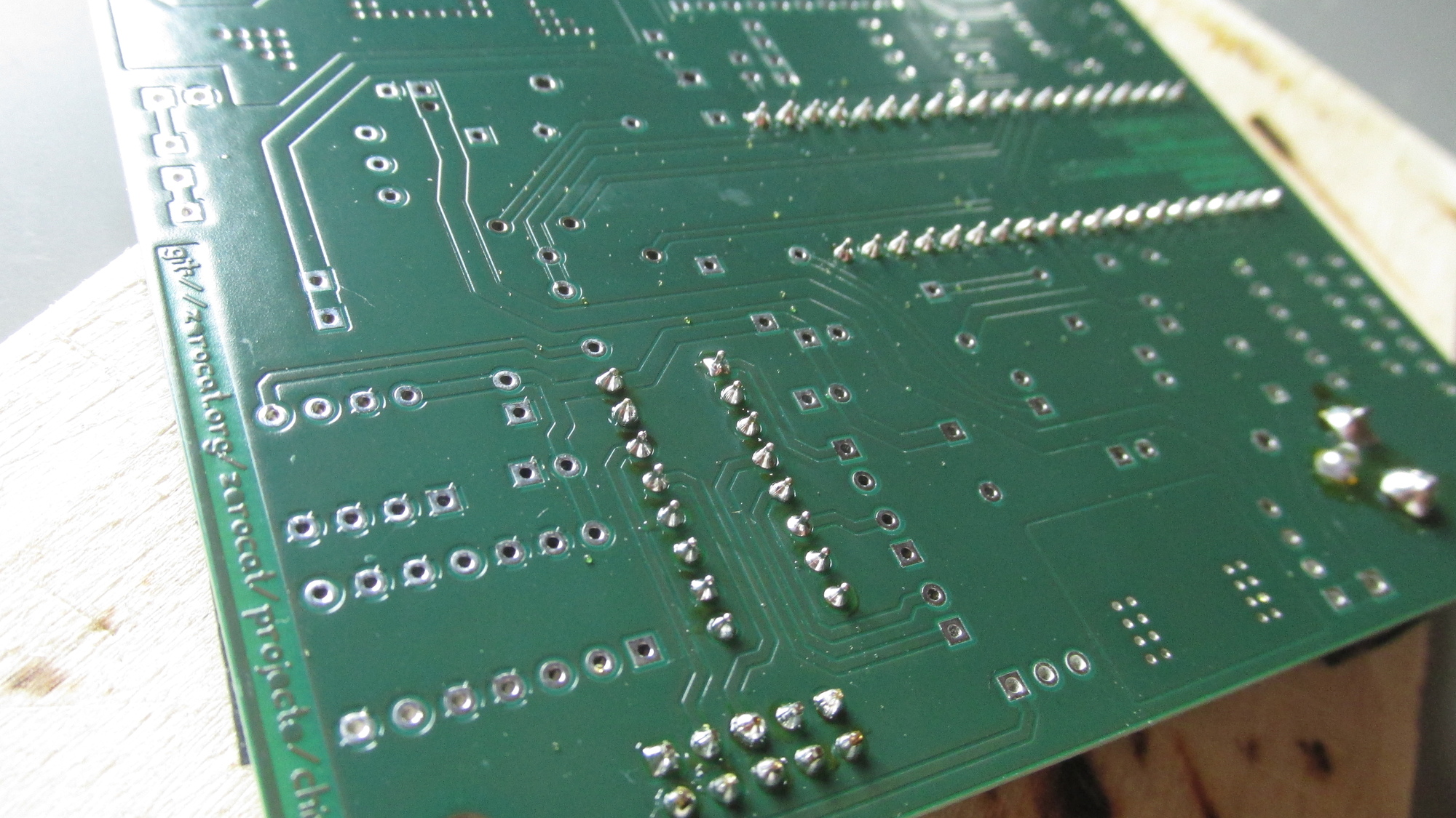
U6 Socket: Done
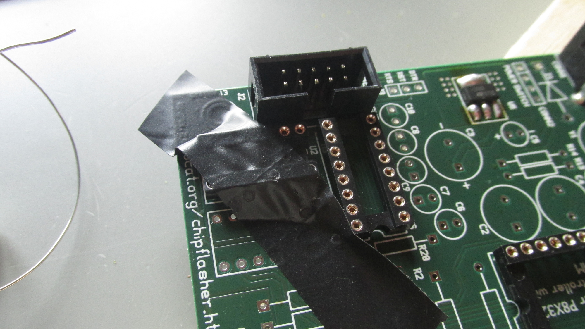
U2 Socket: Place on PCB, fix with tape
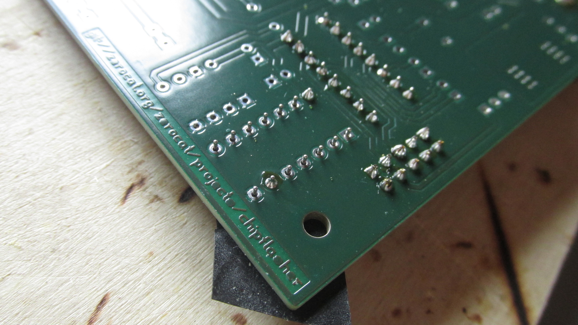
U2 Socket: Solder two diagonal pins, but do not start with thermals!
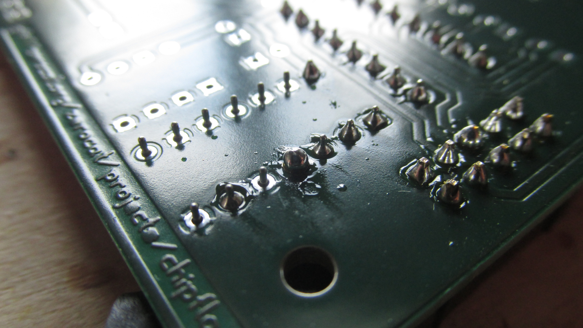
U2 Socket: Thermals are difficult to solder if not hot enough
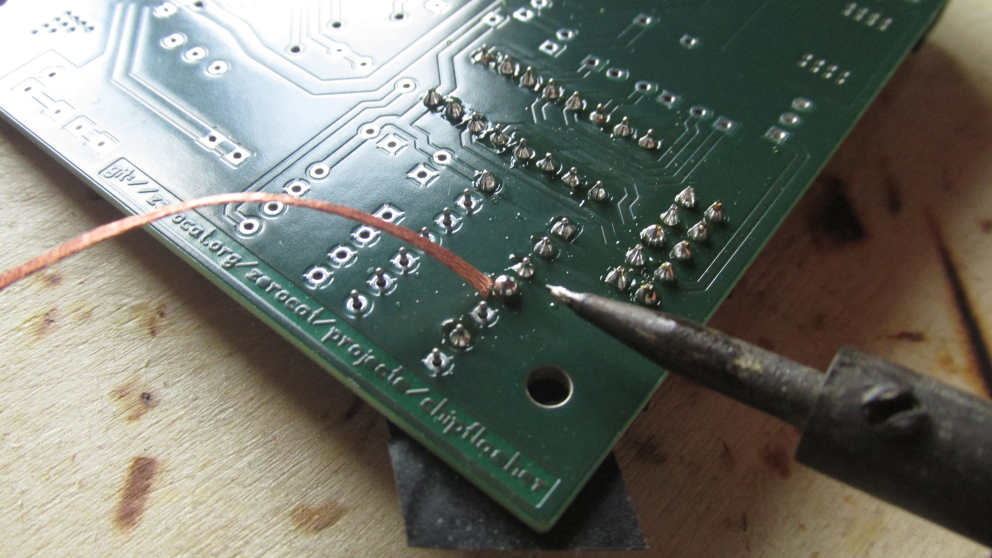
U2 Socket: Remove solder using desolder wire, if available
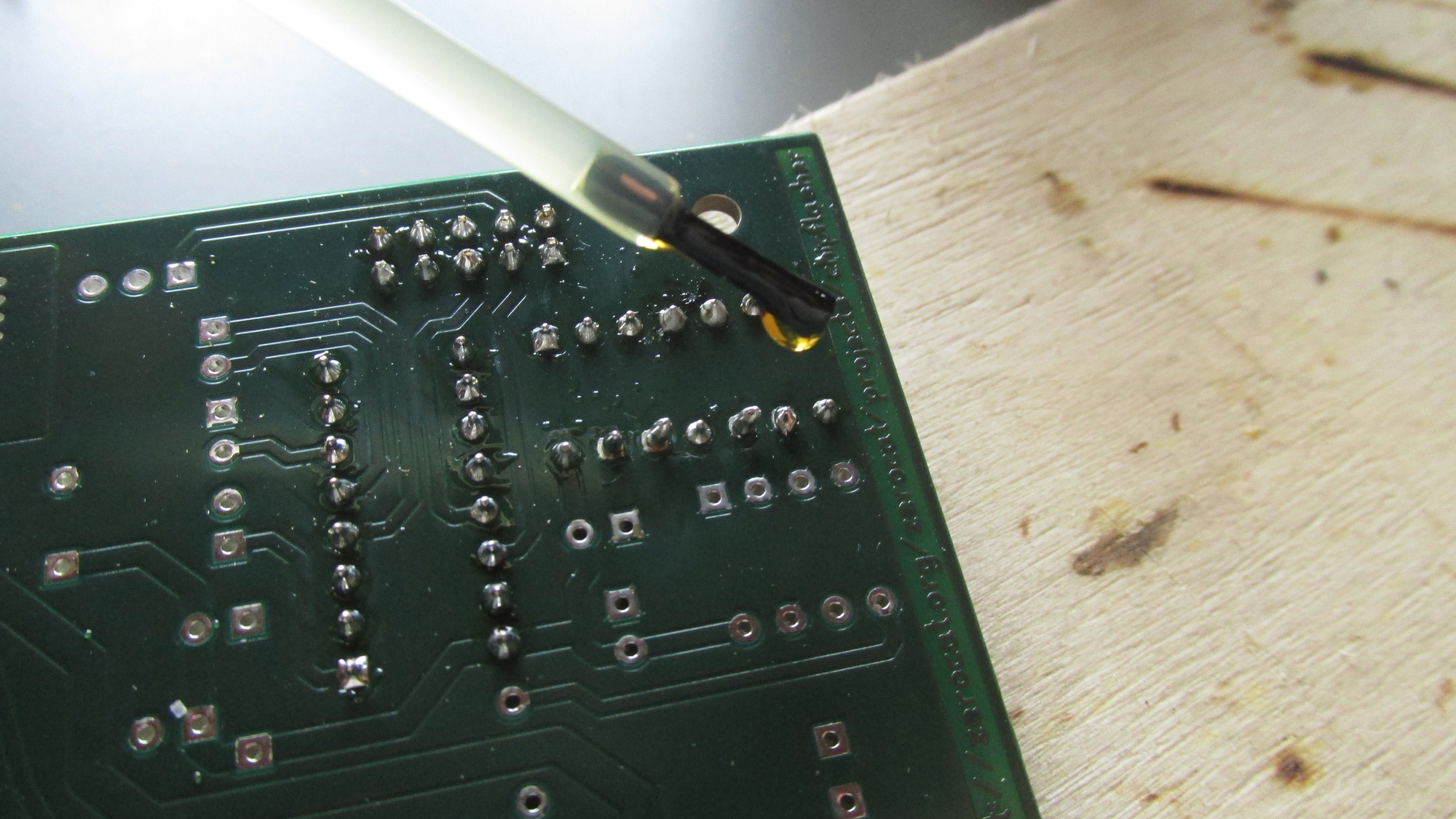
U2 Socket: If available, add resin to ease tin flow
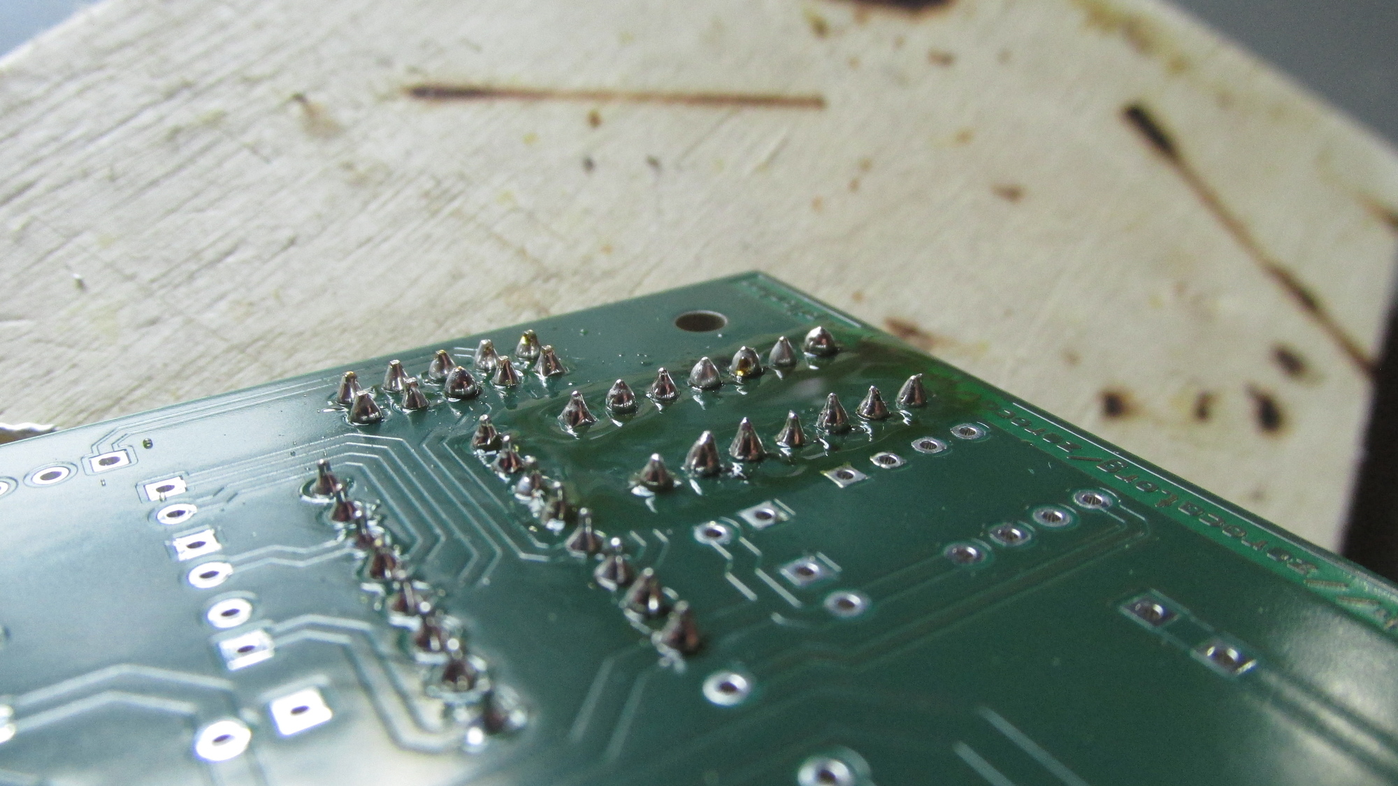
U2 Socket: Be patient with thermals, first add enough heat, then solder.
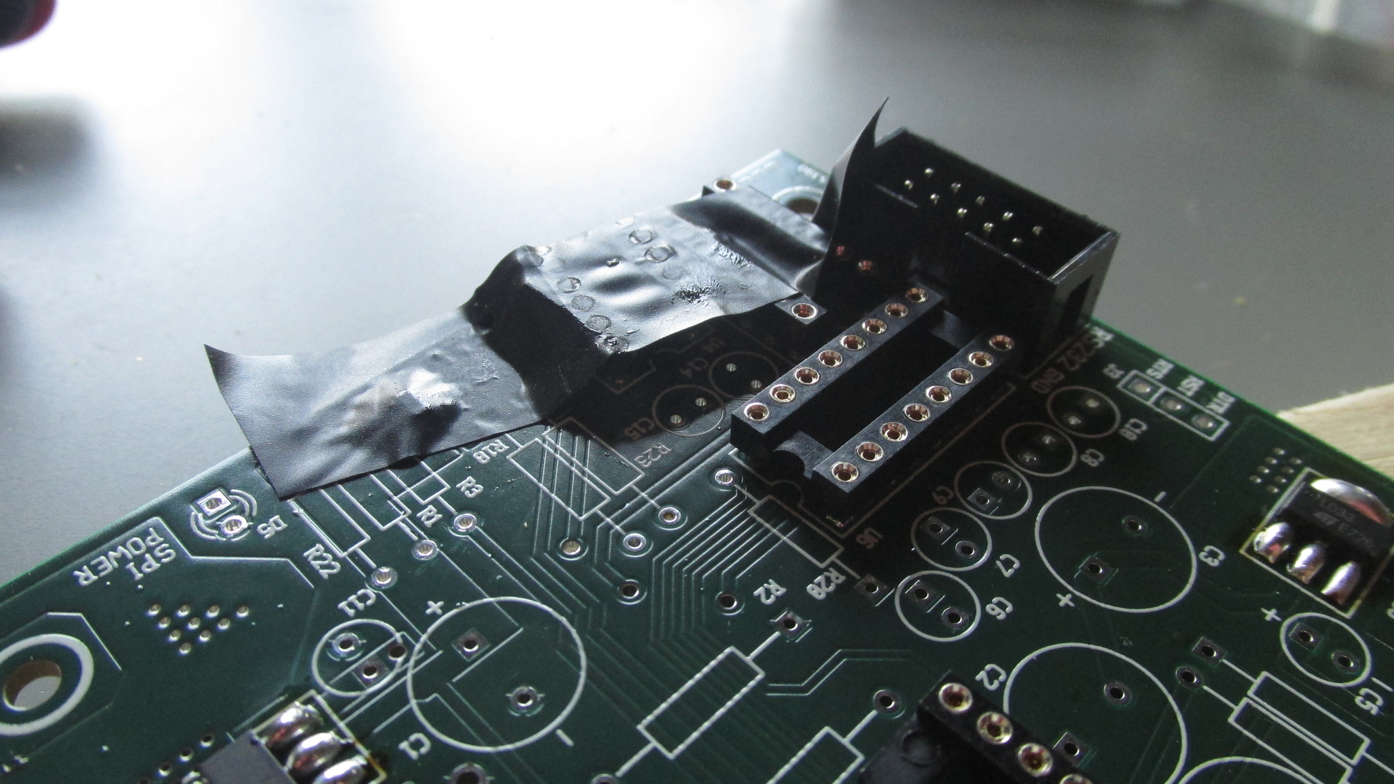
U4 Socket: Place socket on PCB, fix with tape
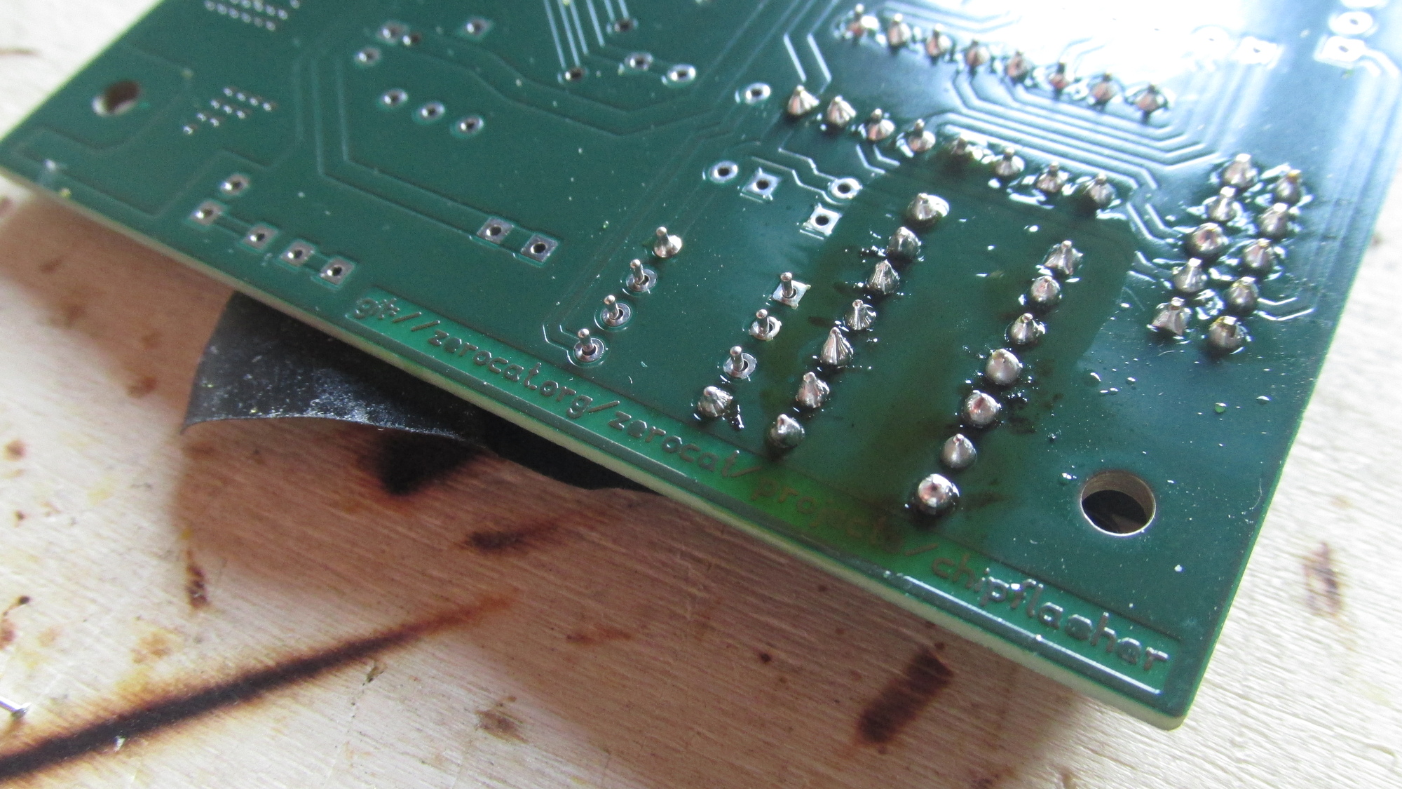
U4 Socket: Solder diagonal pins
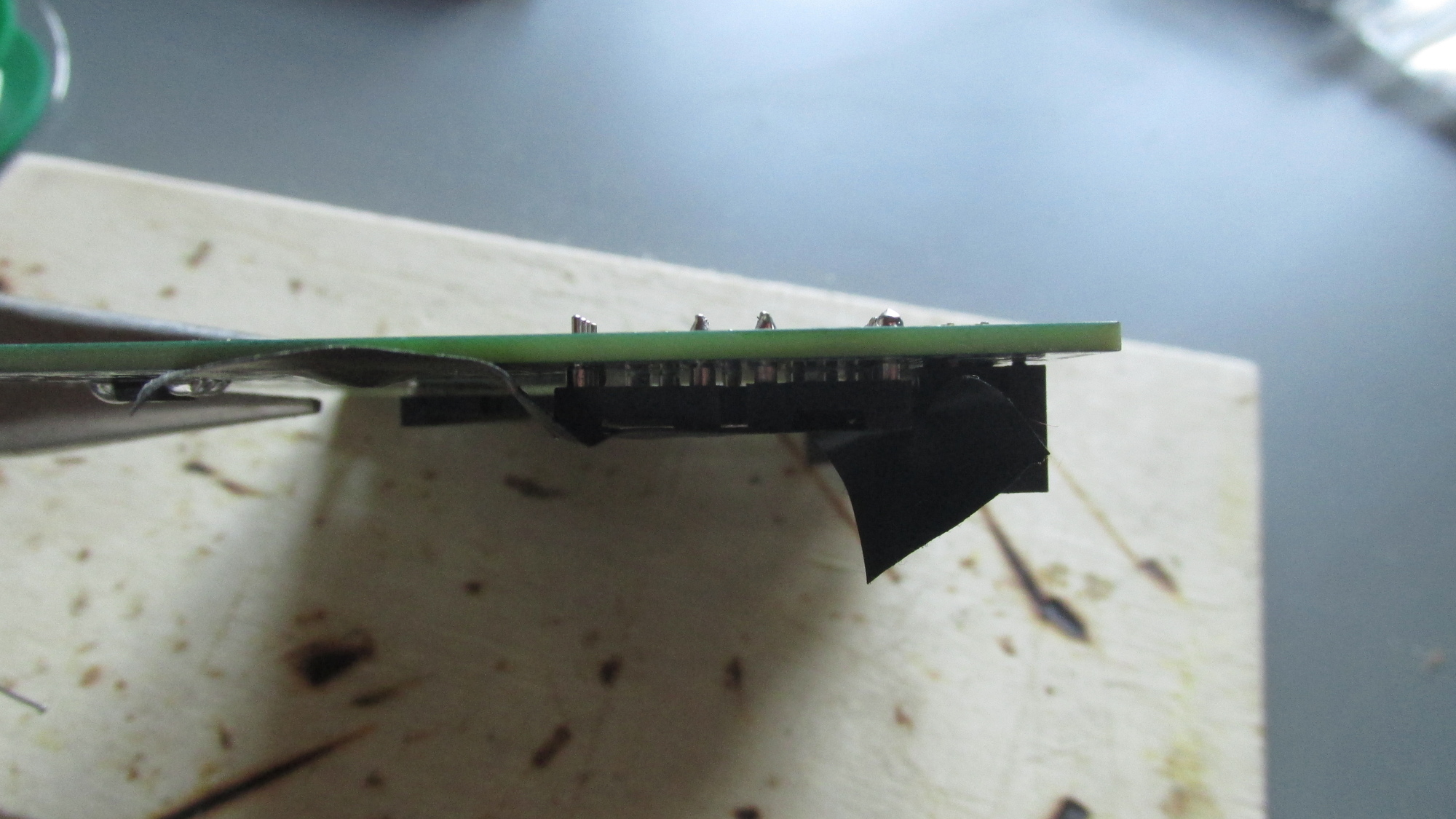
U4 Socket: Check flat position on PCB
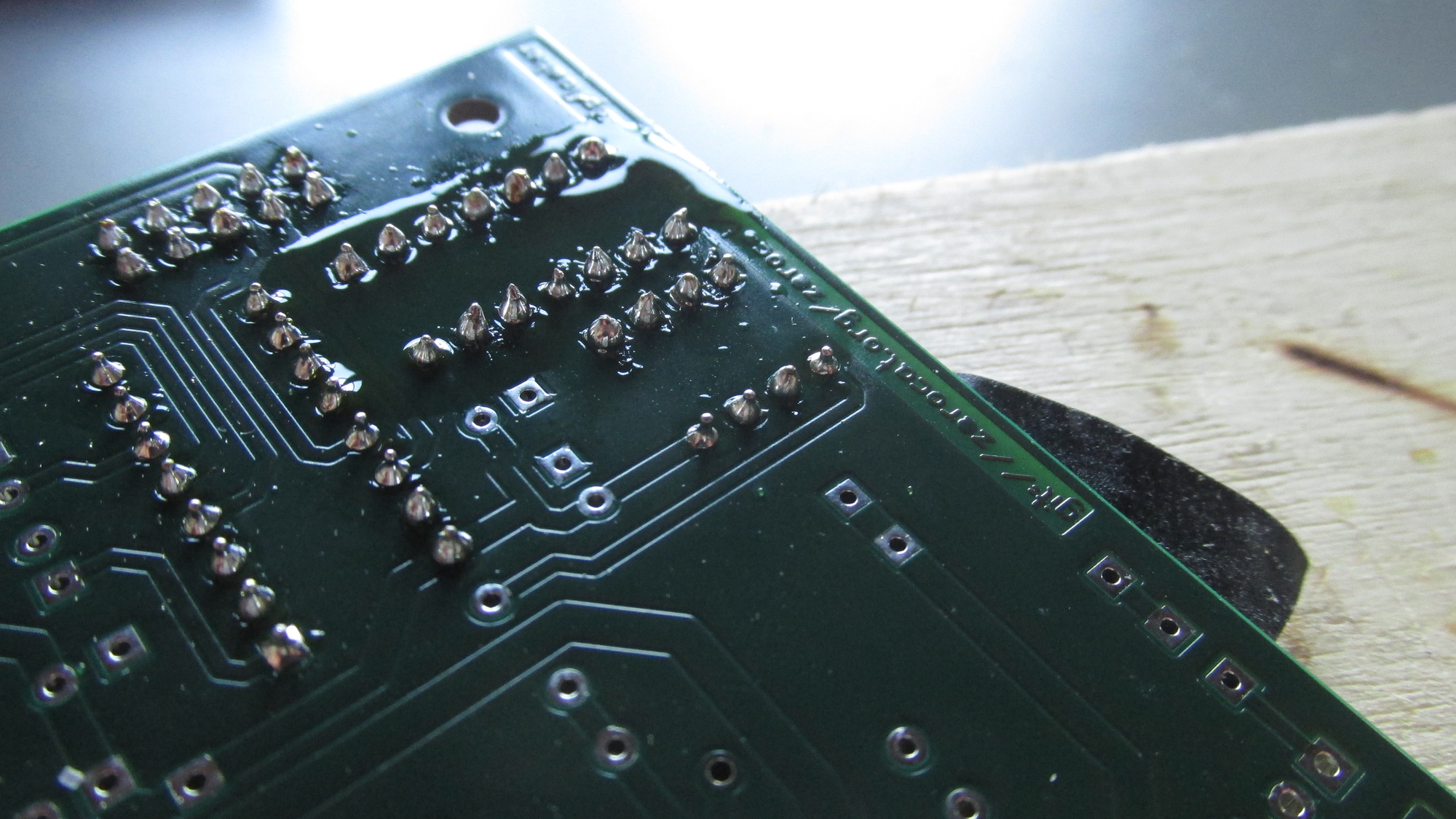
U4 Socket: Solder remaining pins
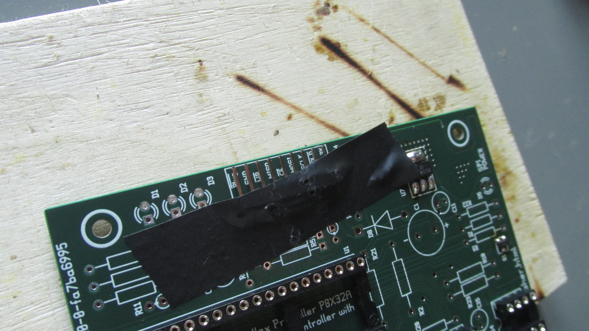
J1: Place 90° pinheader on PCB, fix with tape
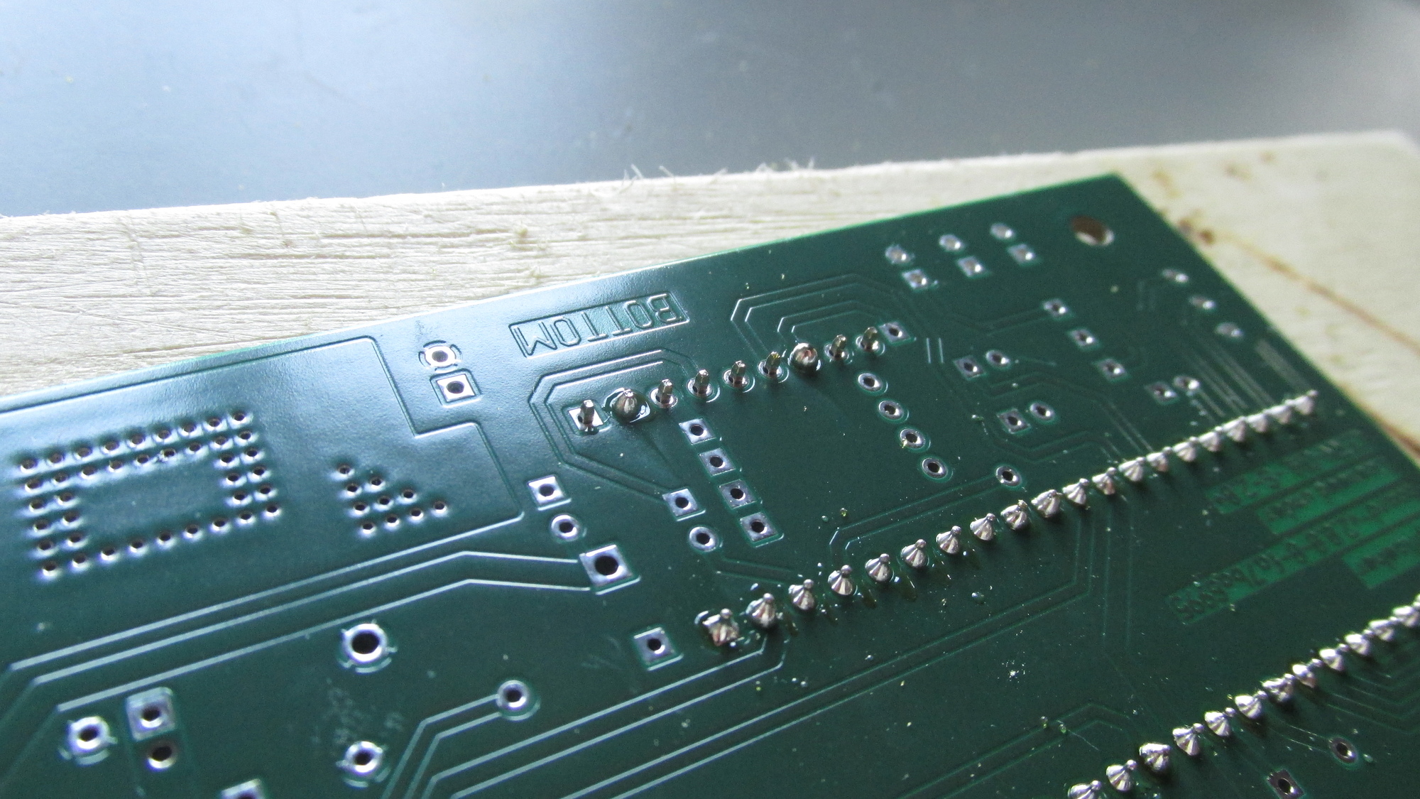
J1: Solder two pins, do not start with thermals
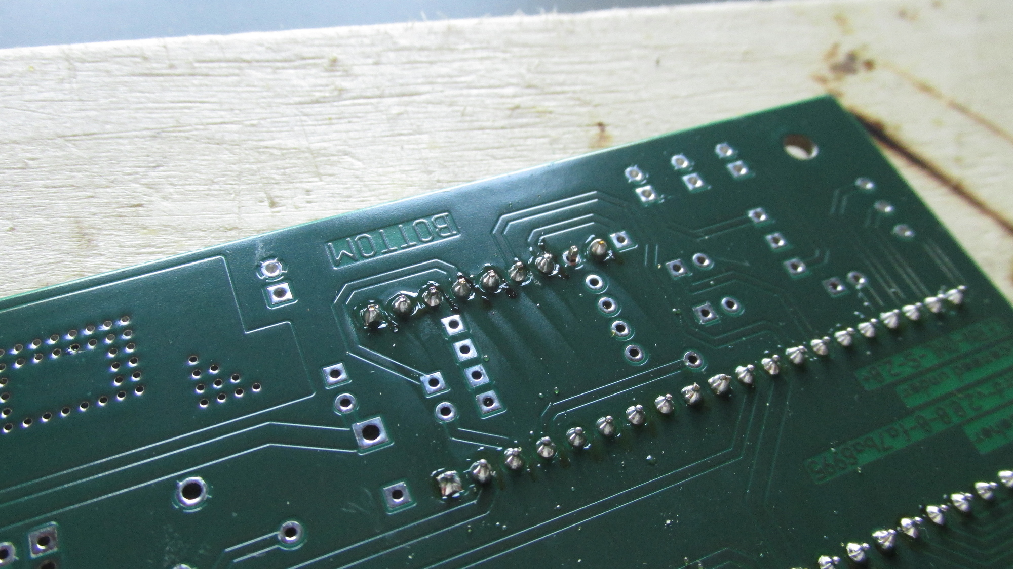
J1: Solder remaining pins except thermal pin
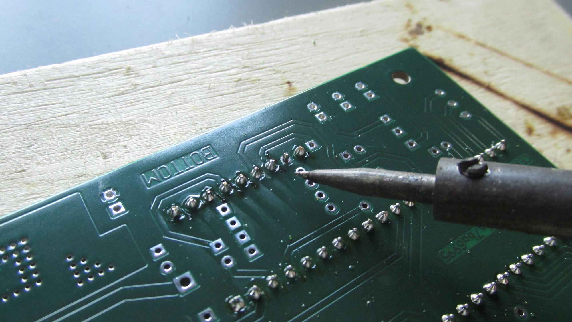
J1: Solder thermal pin, it will heat up slower, be careful that plastic will not melt
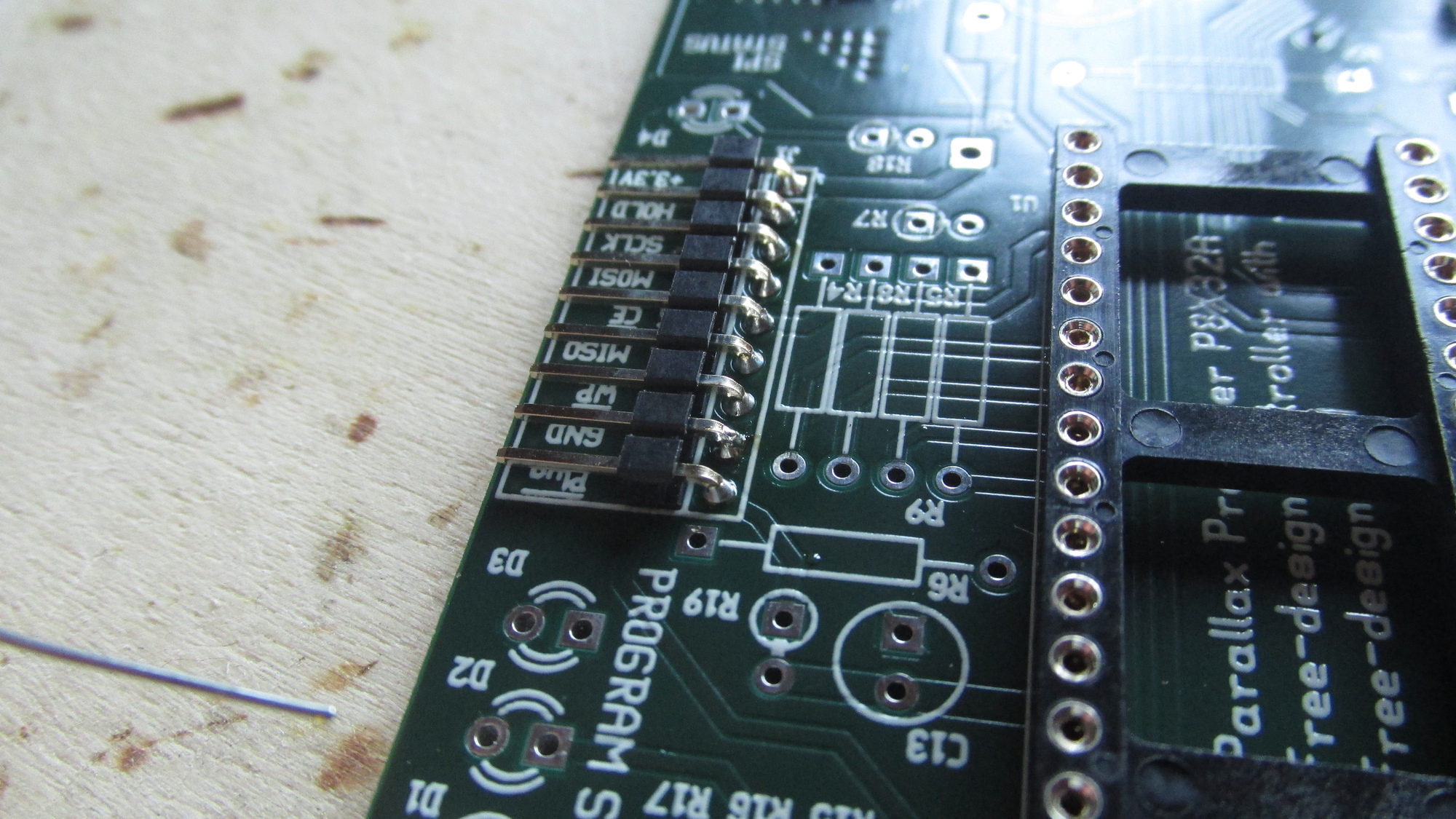
J1: Check solder on component side, fix if required
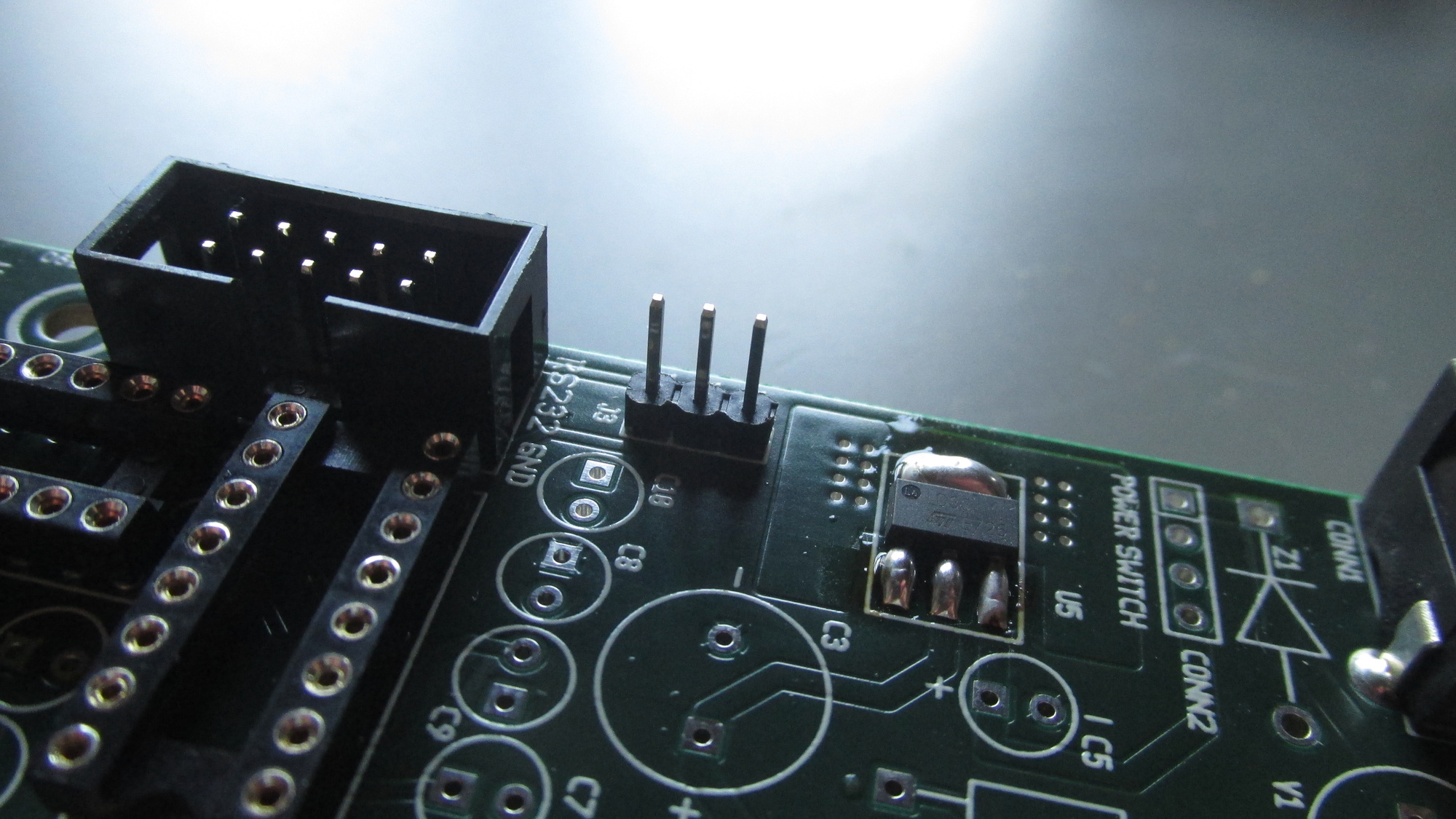
J3: Place pinheader on PCB
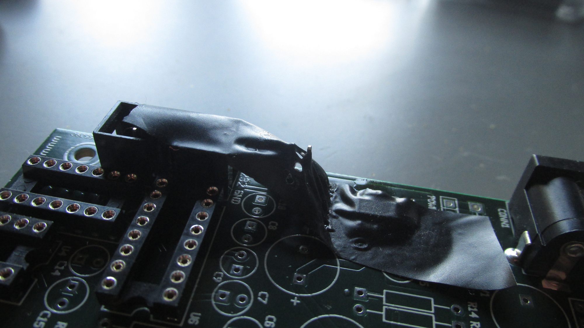
J3: Fix with tape, then solder

CONN2: Place pinheader on PCB, fix with tape, solder one pin
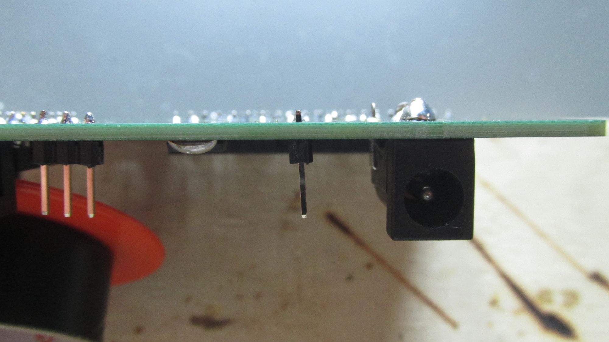
CONN2: Check angle of pinheader, fix if required, solder remaining pins
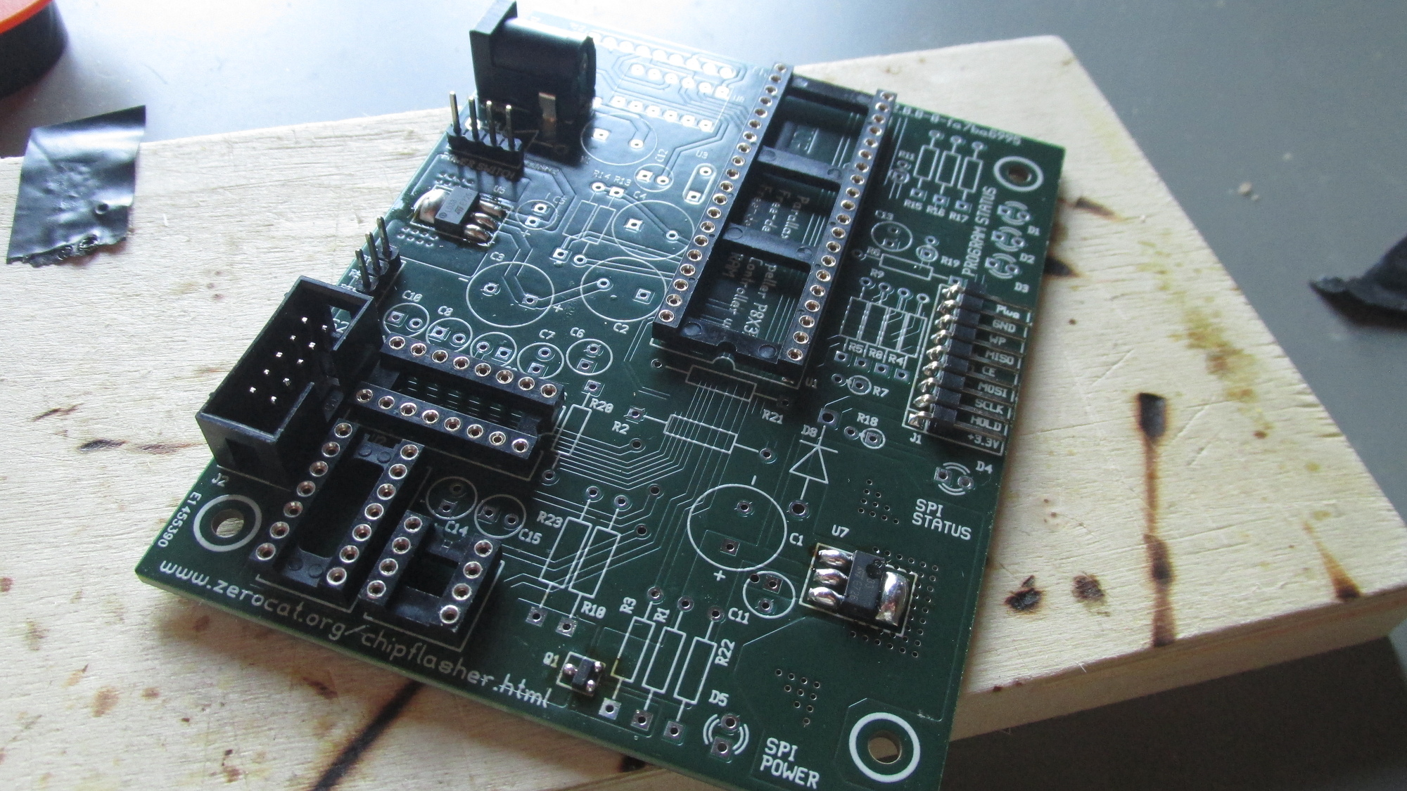
CONN2: We are done with sockets, pinheaders and connectors
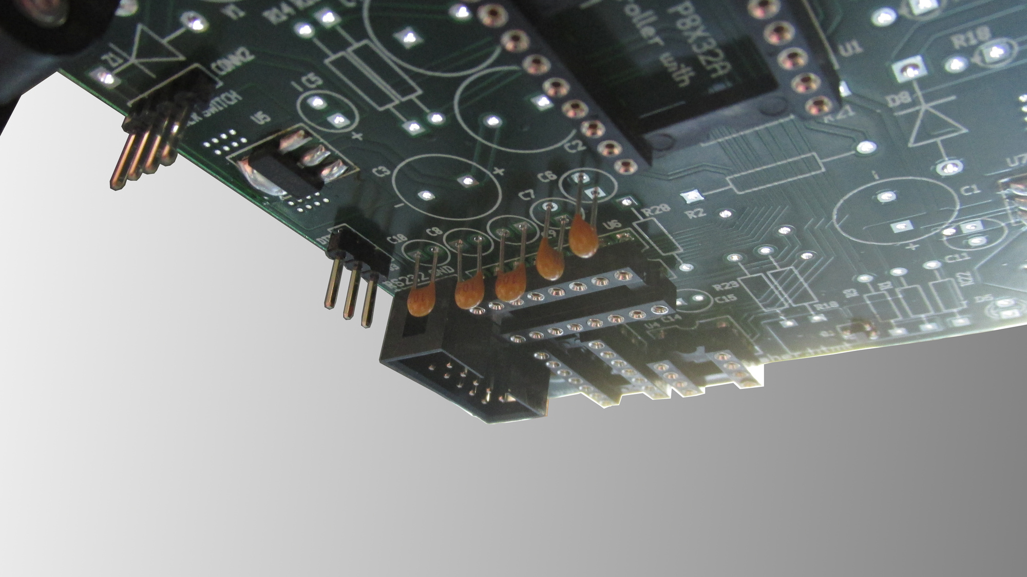
U6 Capacitors: Hold PCB upside down, place U6 capacitors
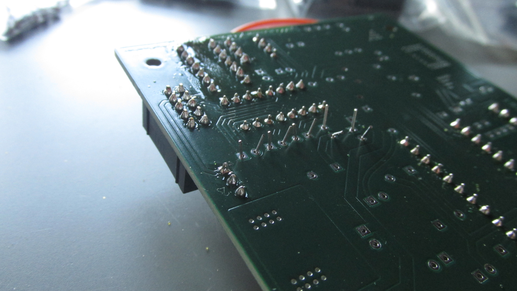
U6 Capacitors: Bent leads such that caps won’t fall
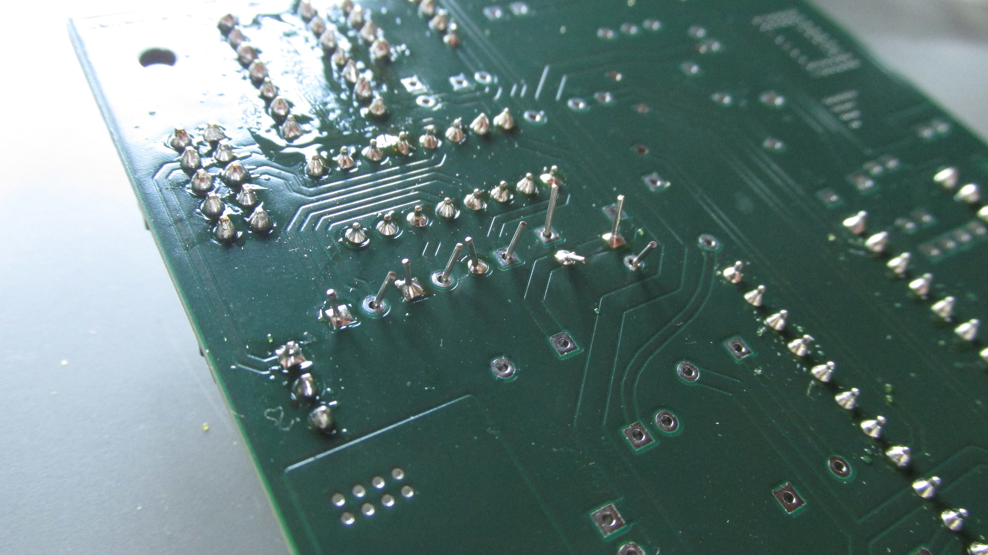
U6 Capacitors: Solder one pin each
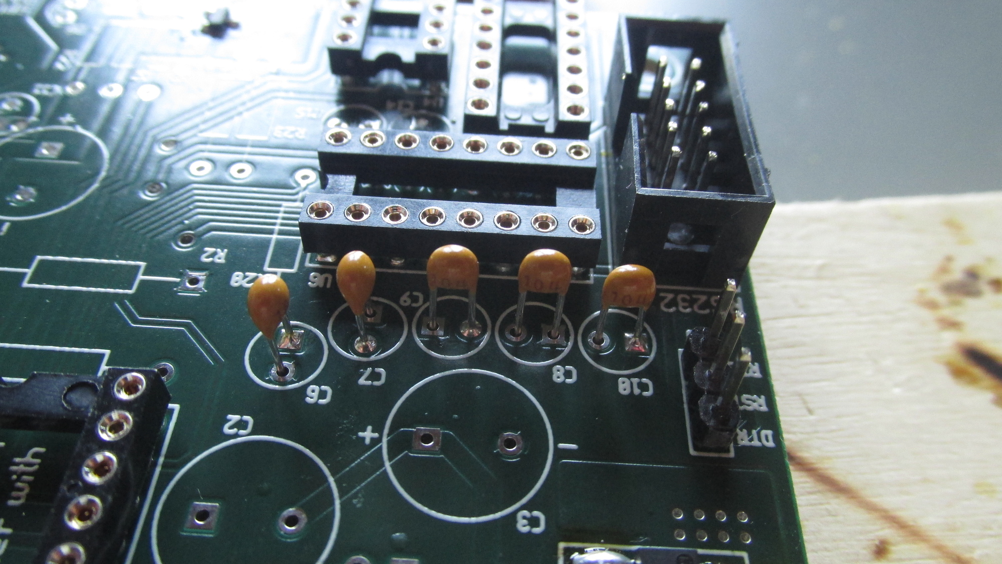
U6 Capacitors: Adjust positions of caps such that they look nice in a row
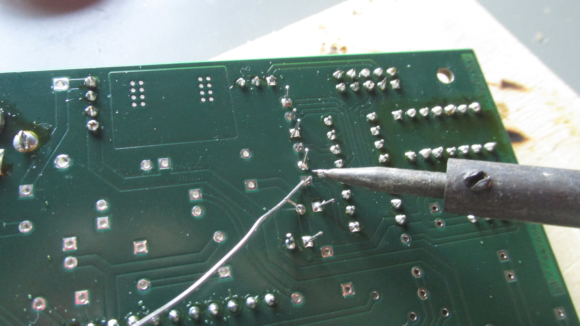
U6 Capacitors: Solder remaining pins
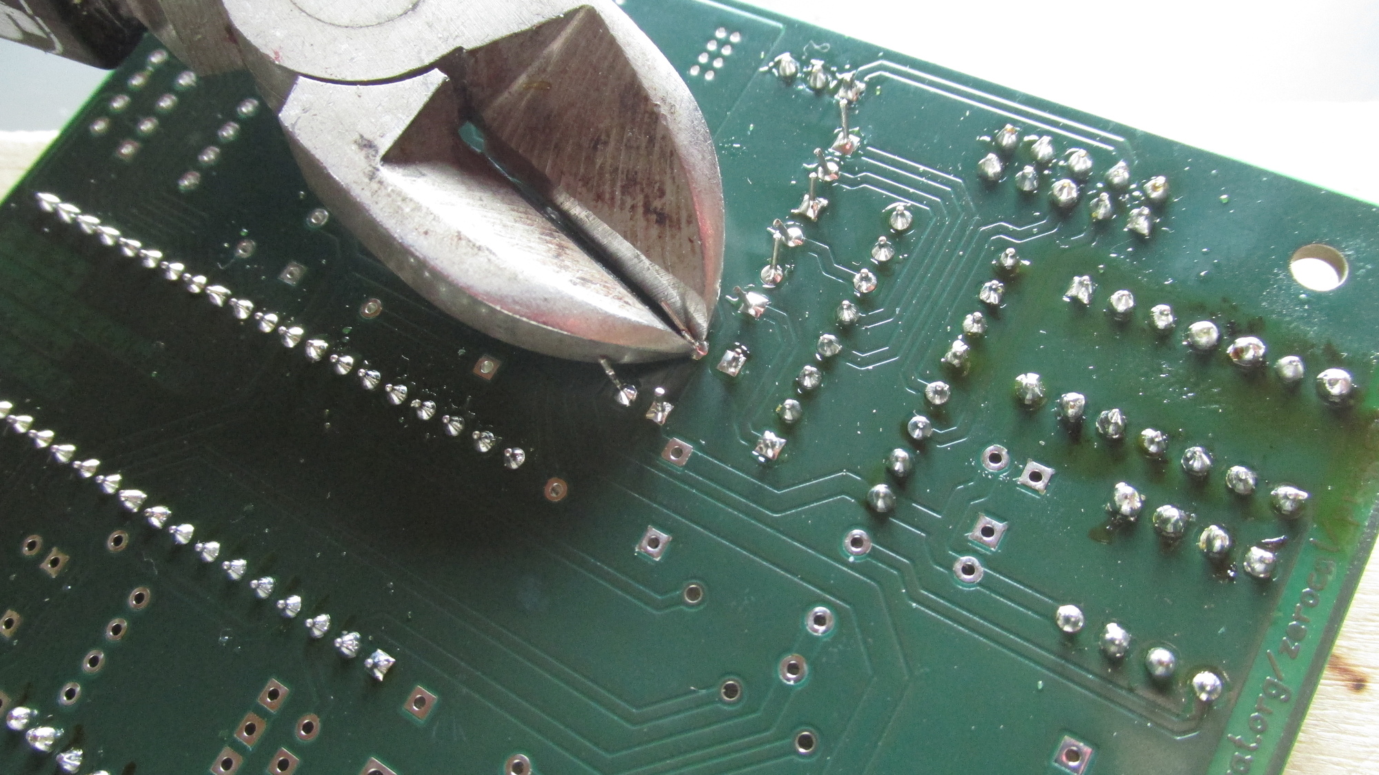
U6 Capacitors: Cut leads
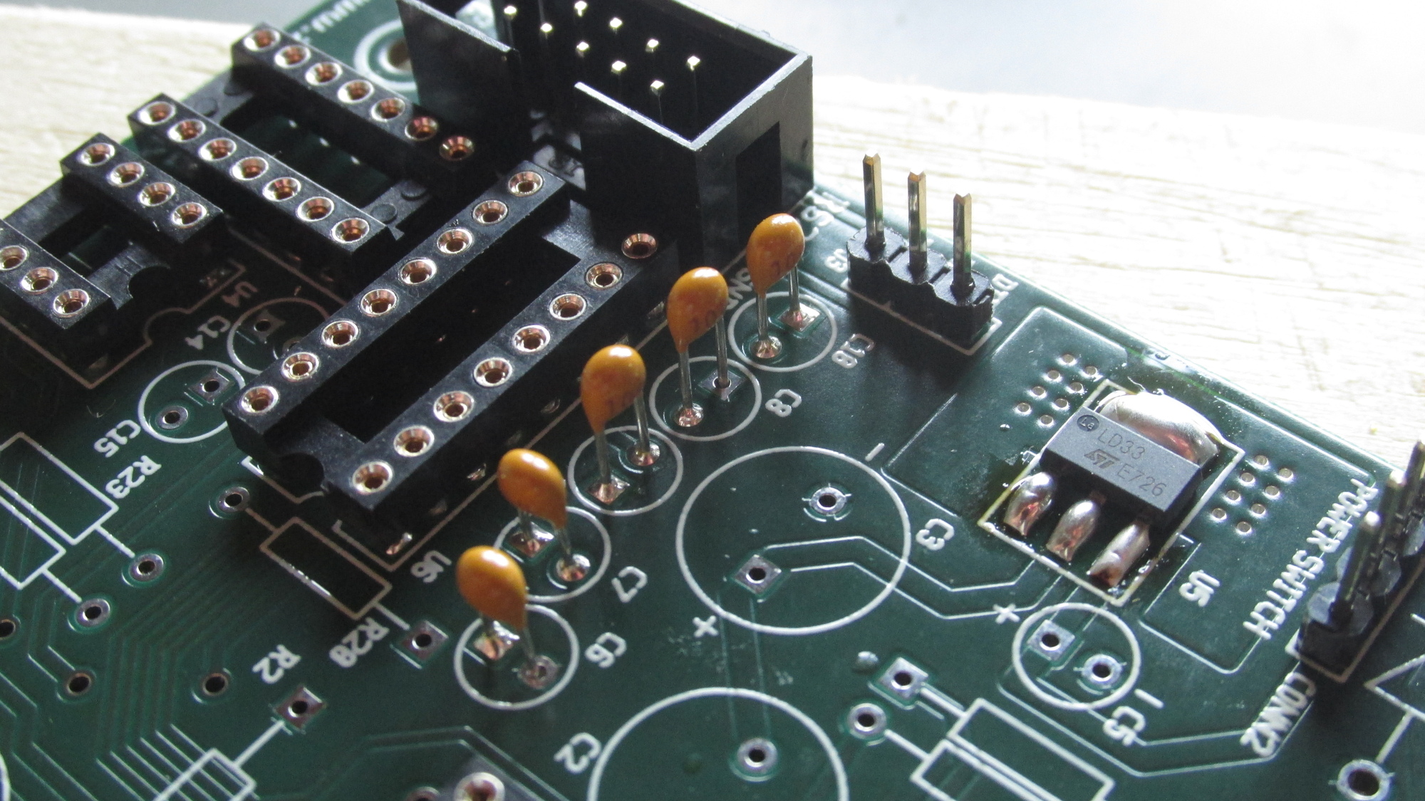
U6 Capacitors: Check pins on component side
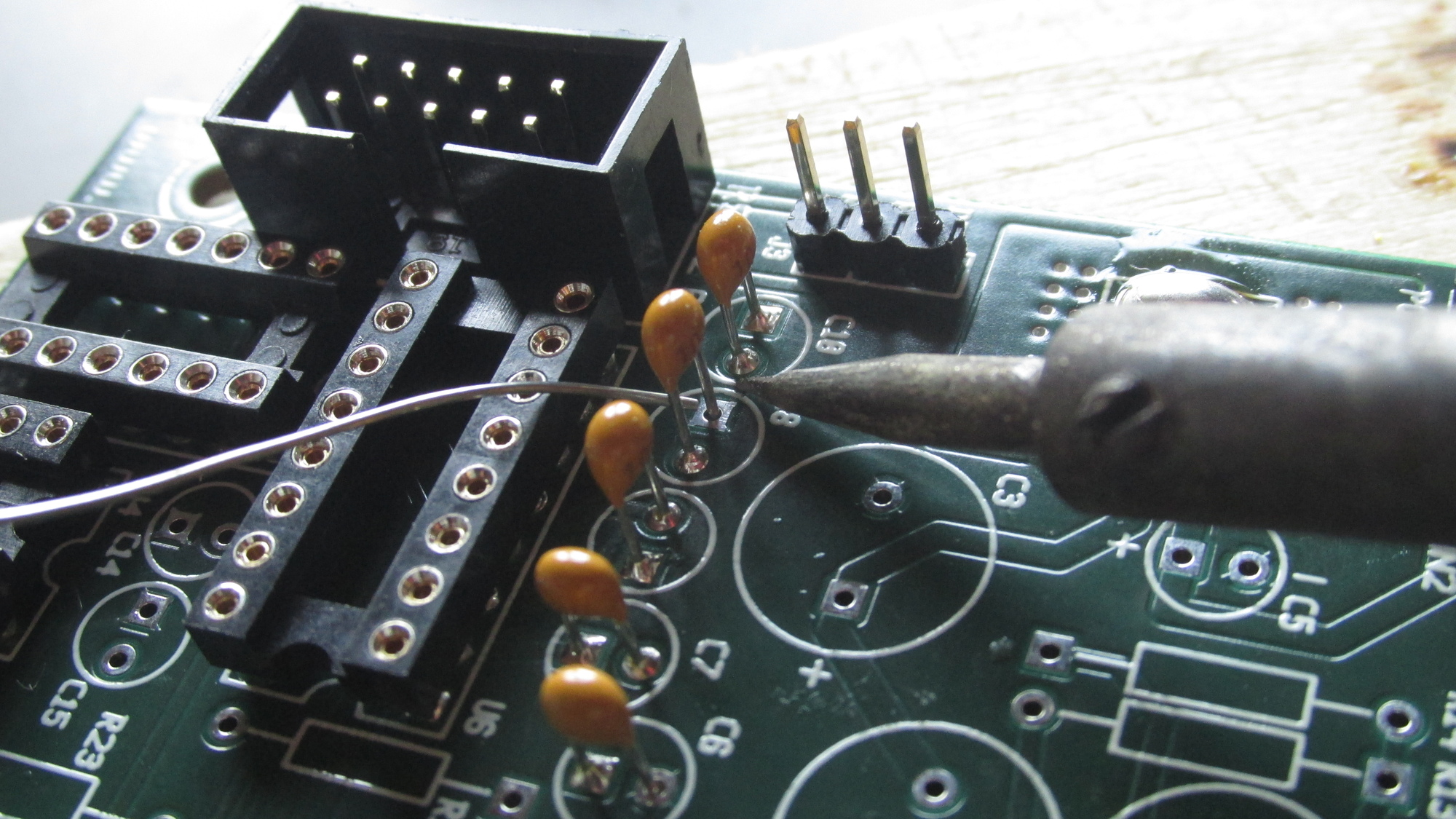
U6 Capacitors: Apply heat and solder where missing
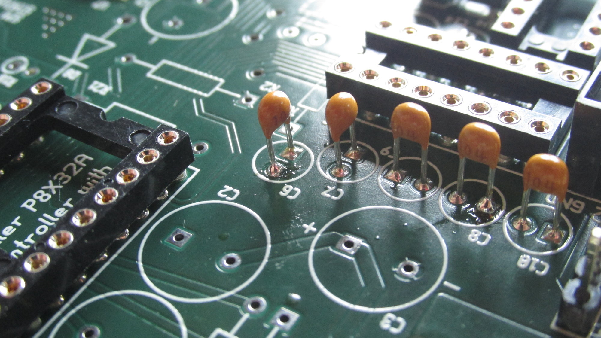
U6 Capacitors: Done
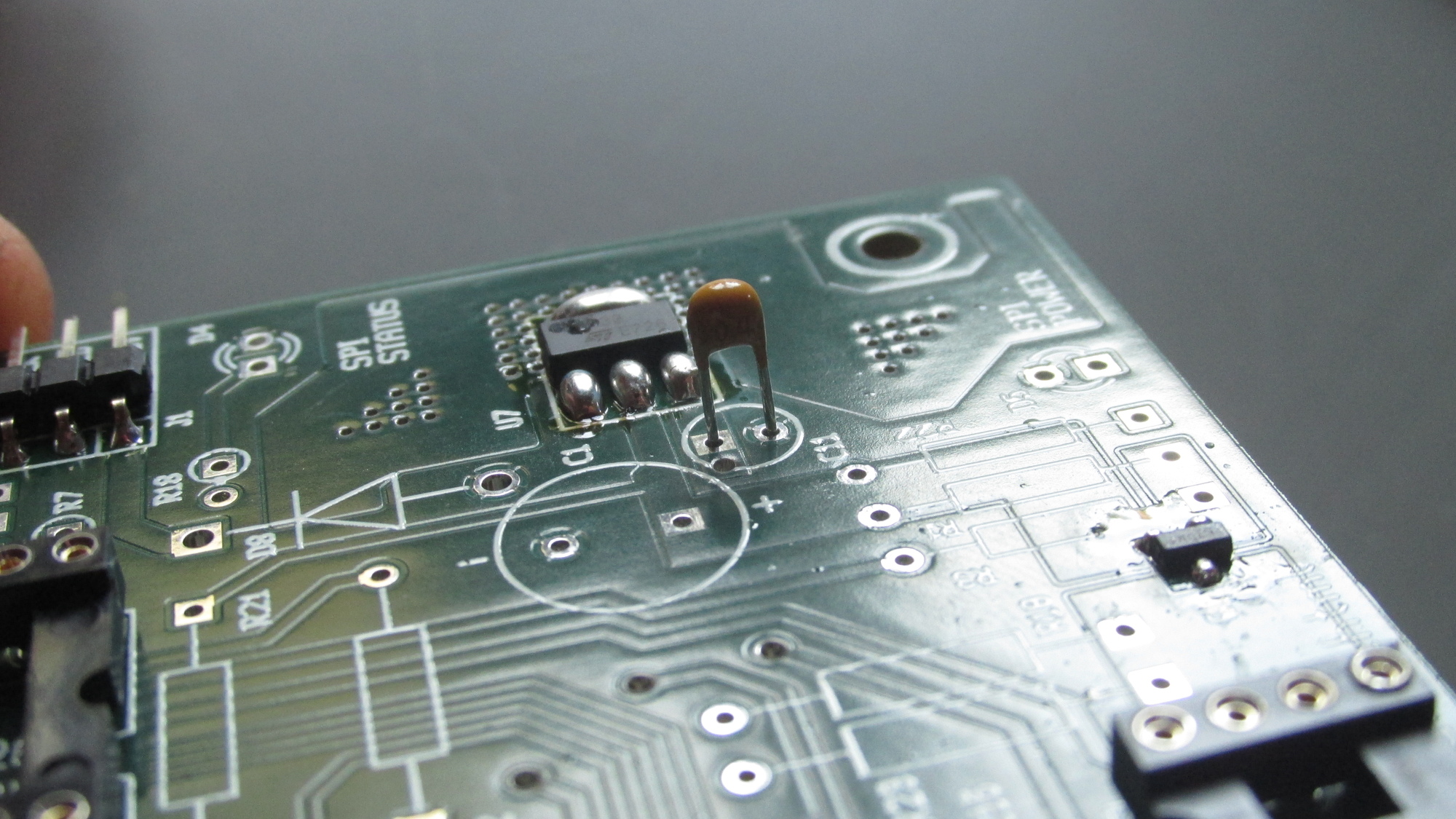
C11: Place capacitor on PCB
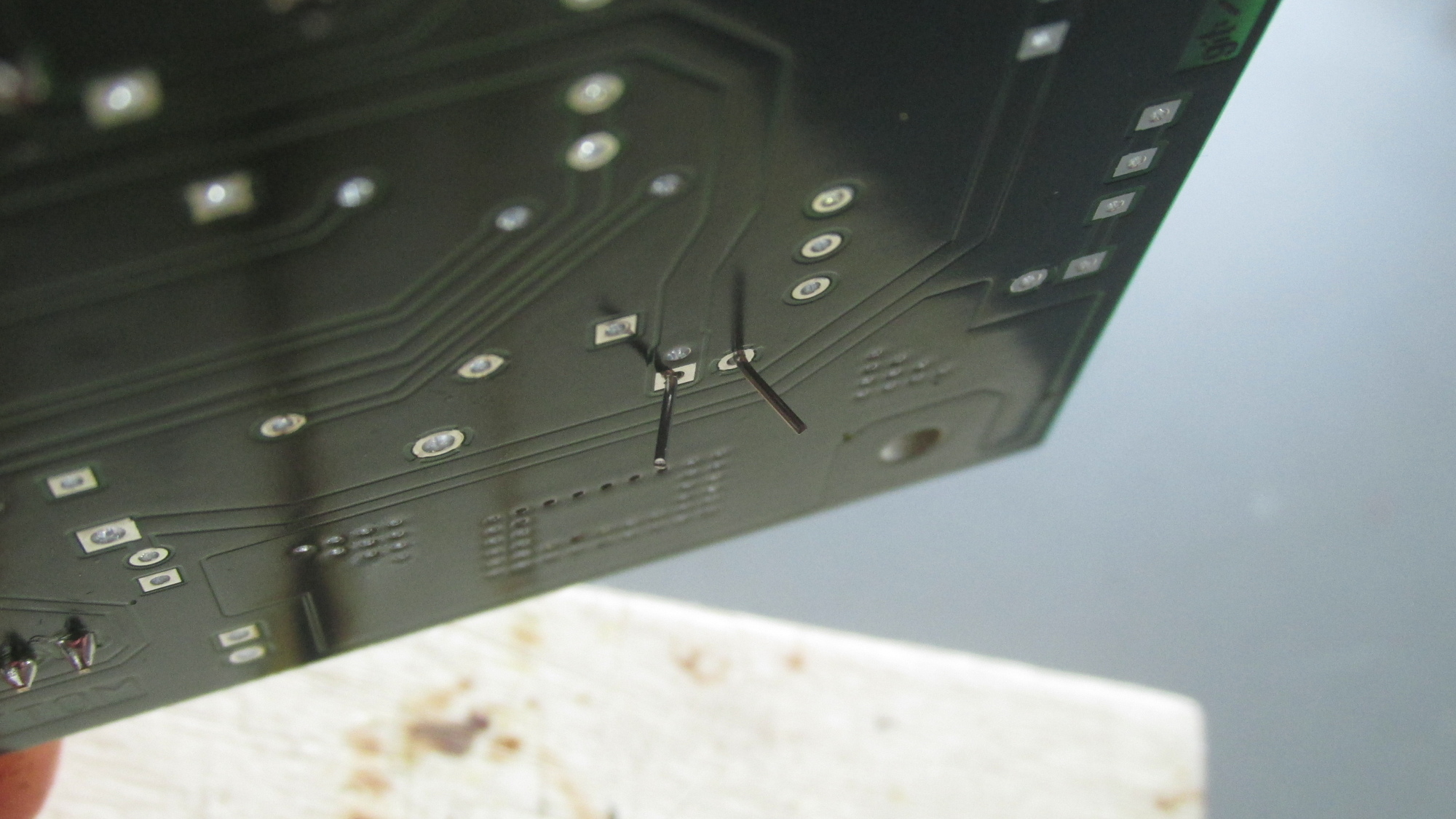
C11: Bent leads such that it remains in place
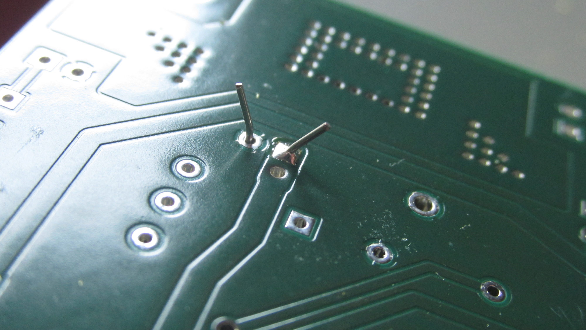
C11: Solder pin well to ensure electrical connection of top and bottom power routes
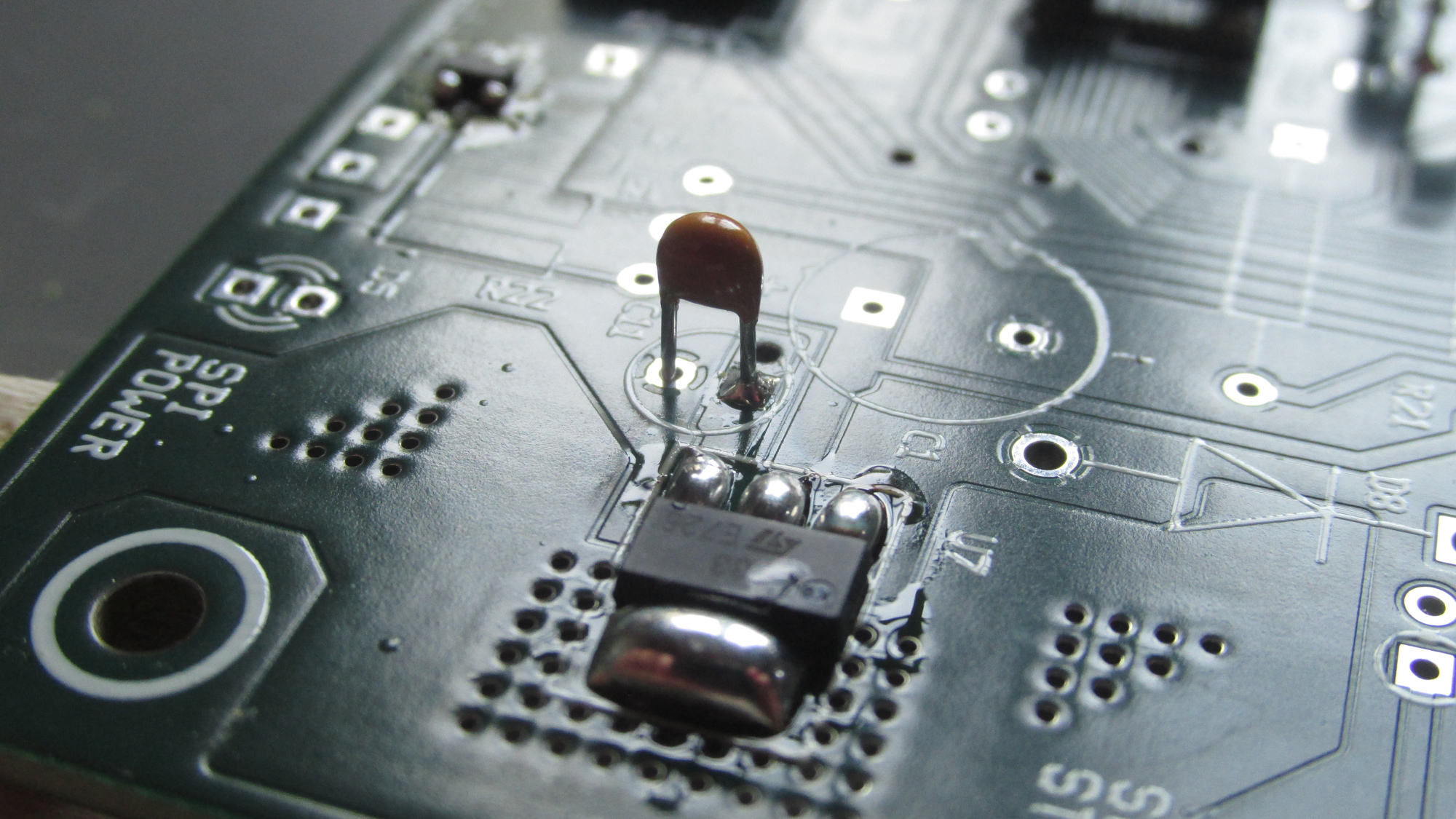
C11: Fix solder on component side if required, adjust position
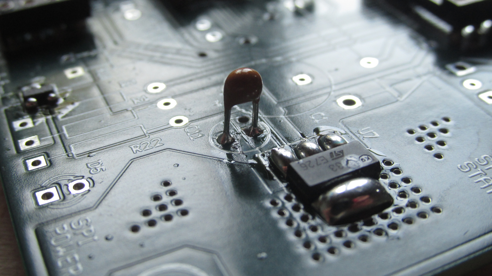
C11: Solder thermal pin well, it will heat up like 3 to 5 times slower
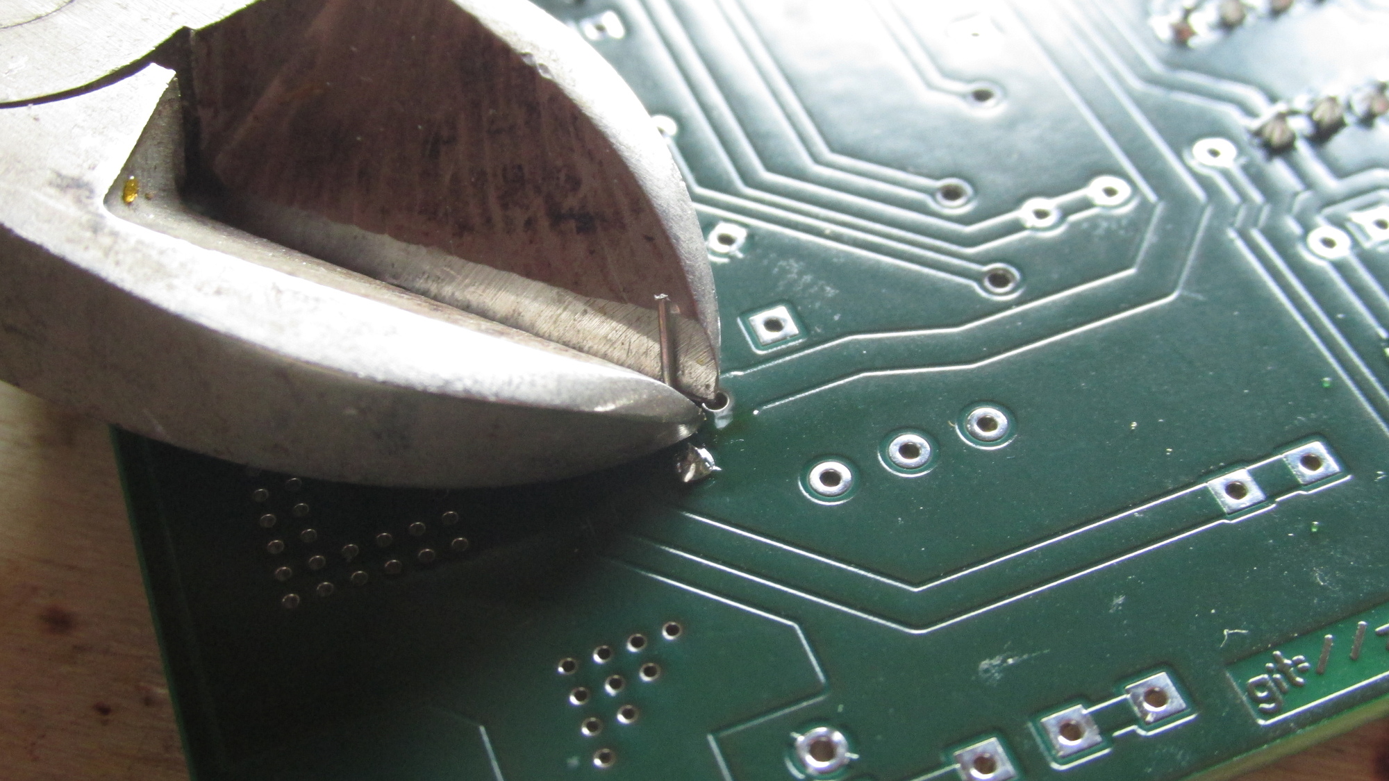
C11: Cut leads
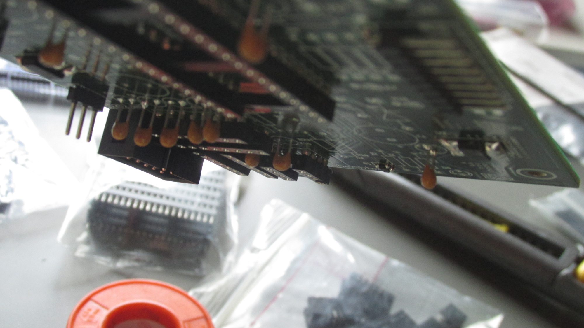
C12, C13, C14, C15: Flip PCB upside down, place capacitors on PCB
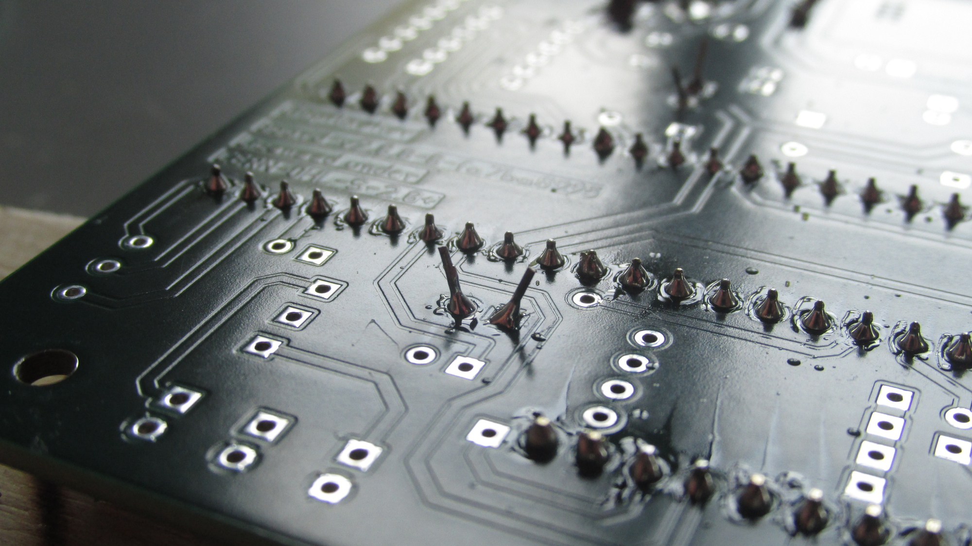
C12, C13, C14, C15: Bent leads such that they remain in place, solder pins, cut leads
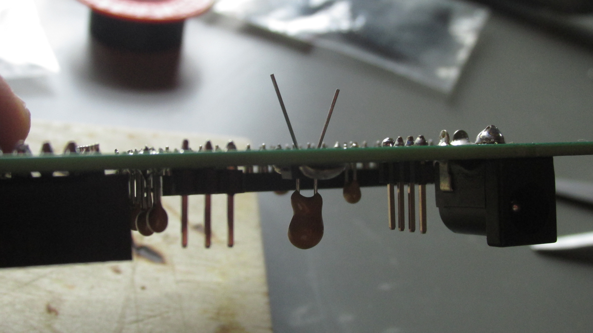
C5: Flip PCB upside down, place capacitor, bent leads
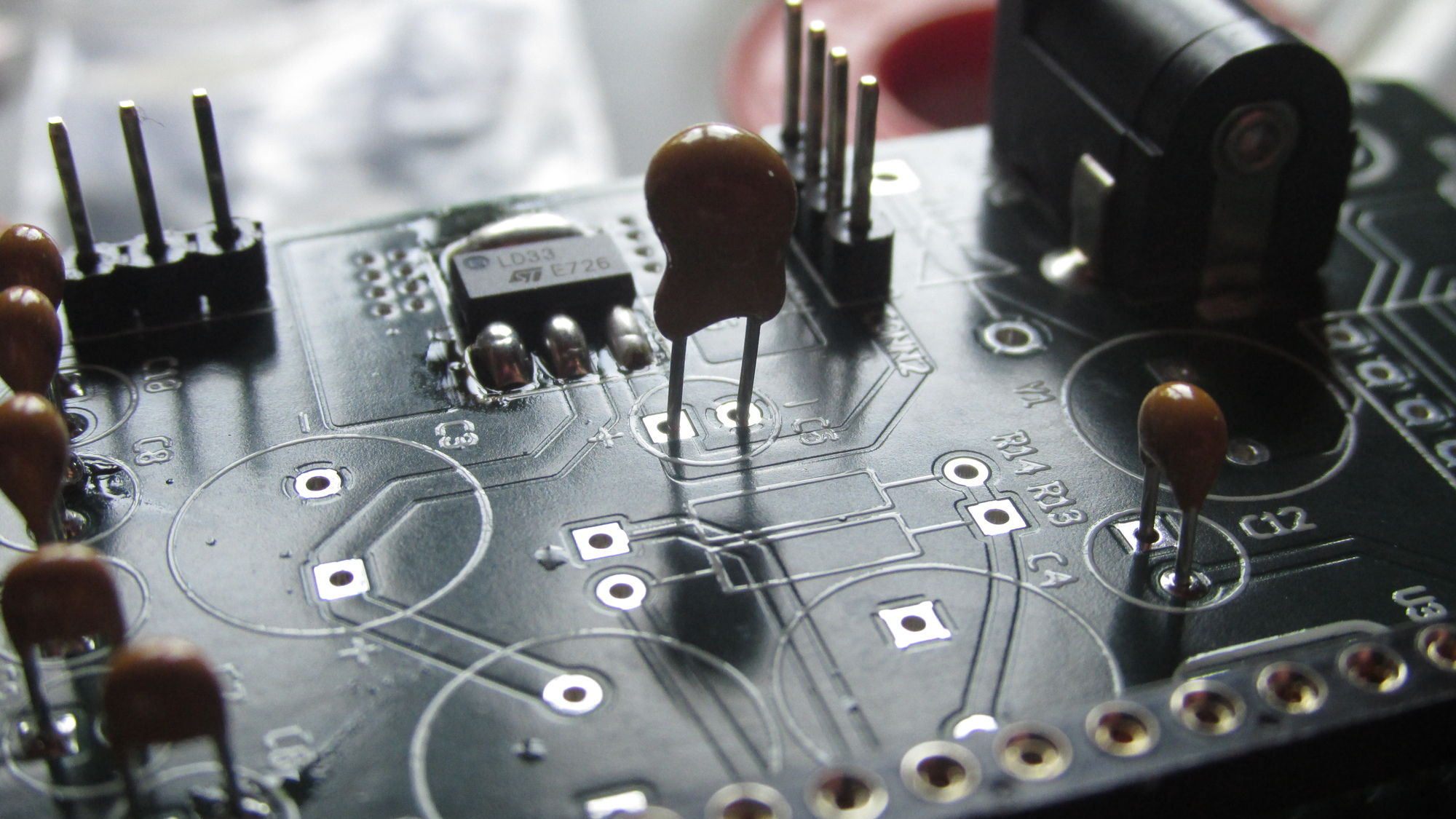
C5: Check polarity: Thermal pad must be connected with shorter lead!
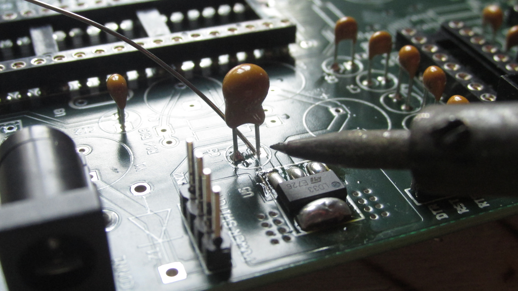
C5: Solder pins on both sides, cut leads
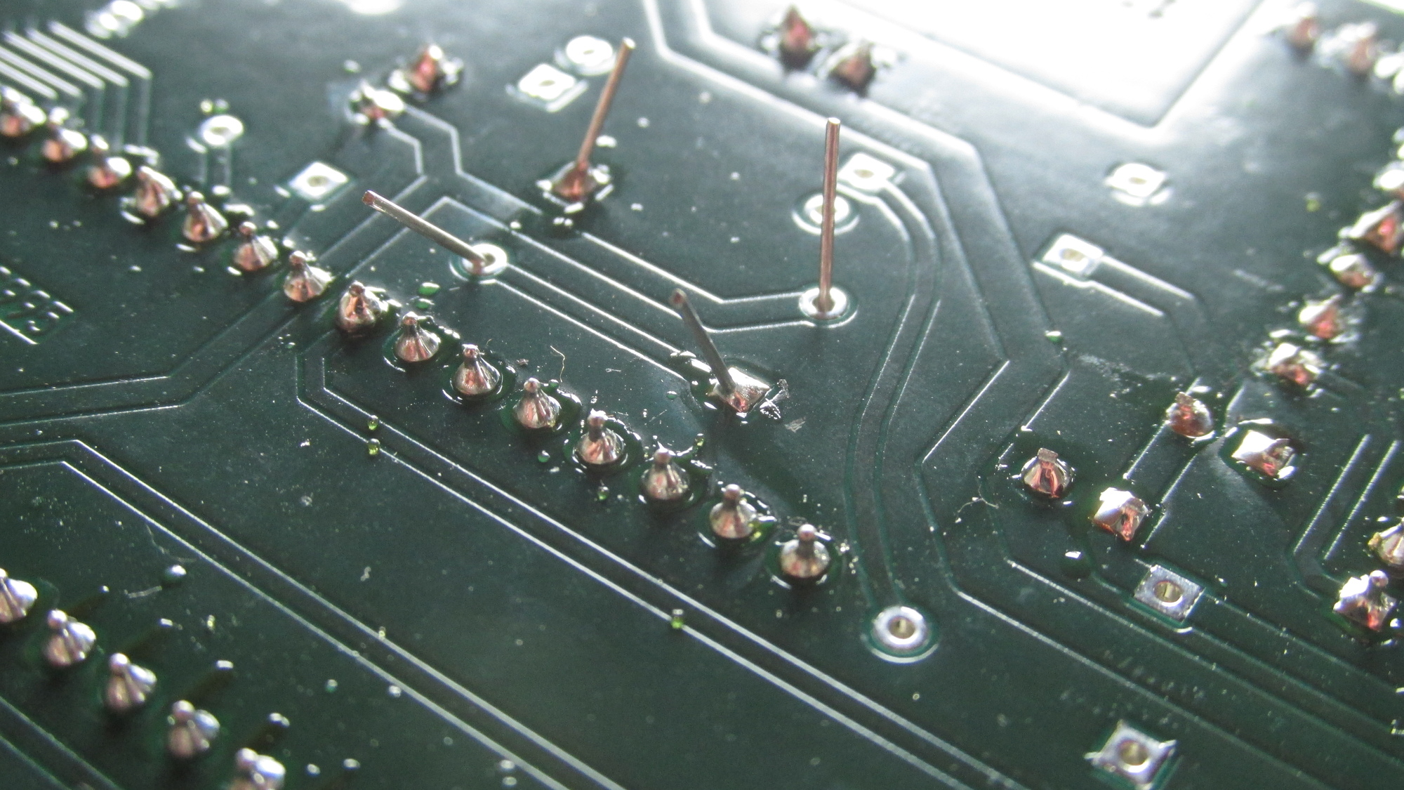
C2, C4: Flip PCB upside down, place capacitors, bent leads, solder one pin each
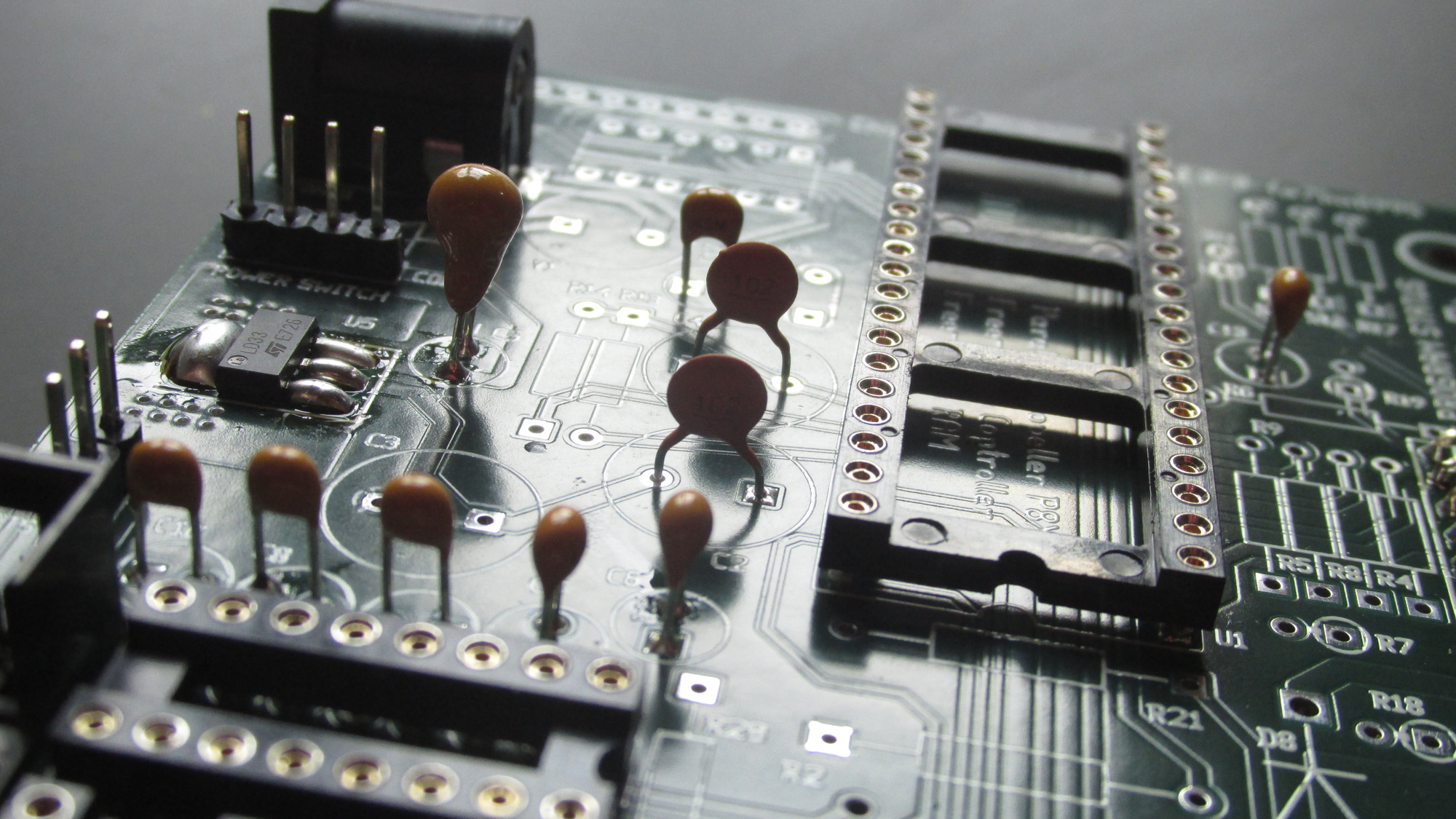
C2, C4: Adjust positions
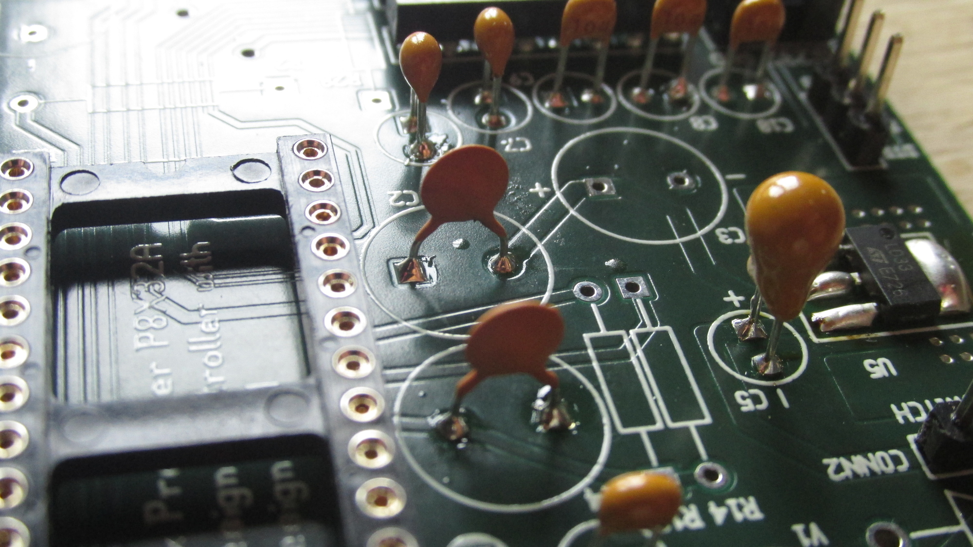
C2, C4: Solder pins on both PCB sides, cut leads
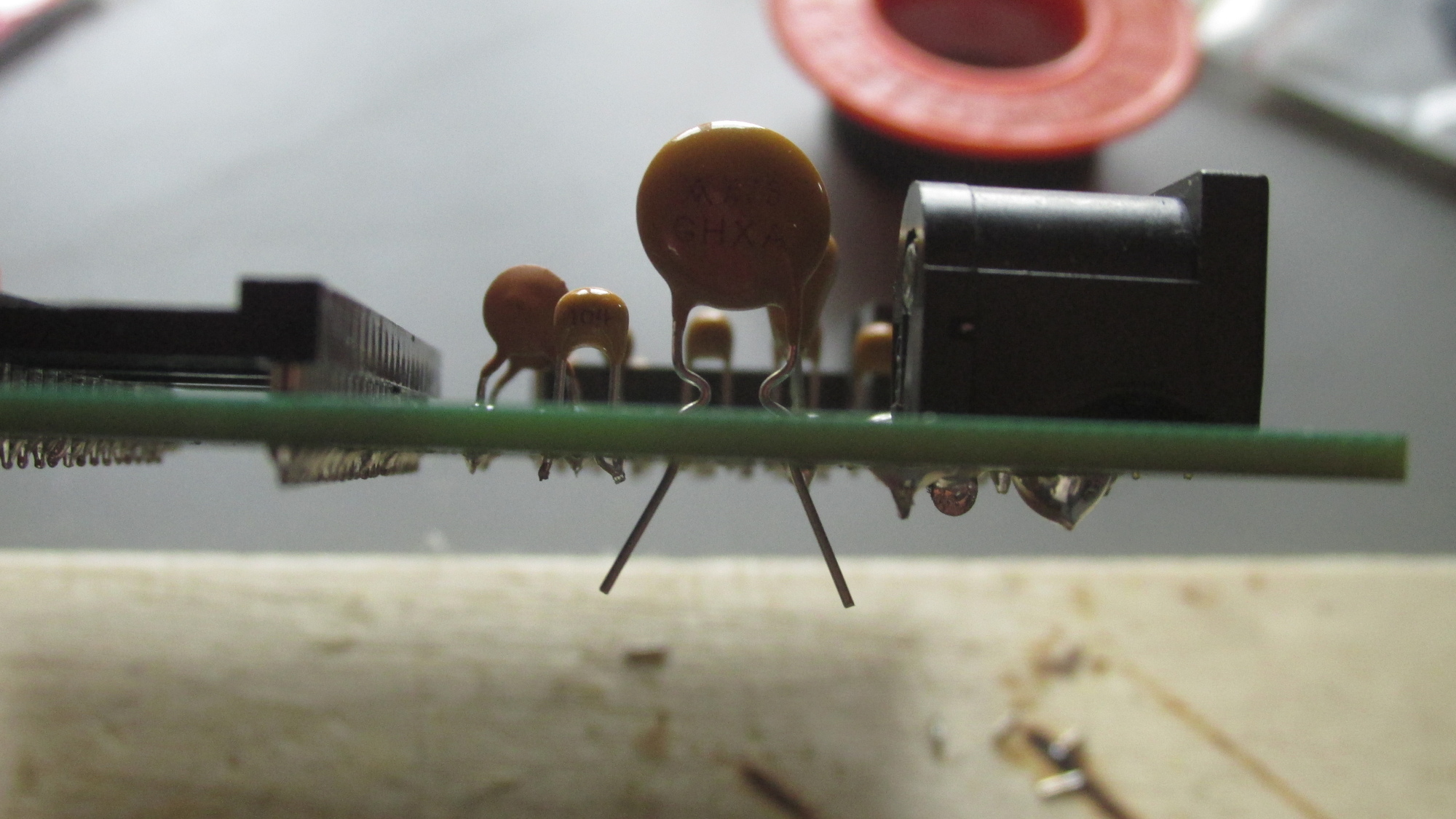
V1: Place fuse on PCB, bent leads such that it remains in place
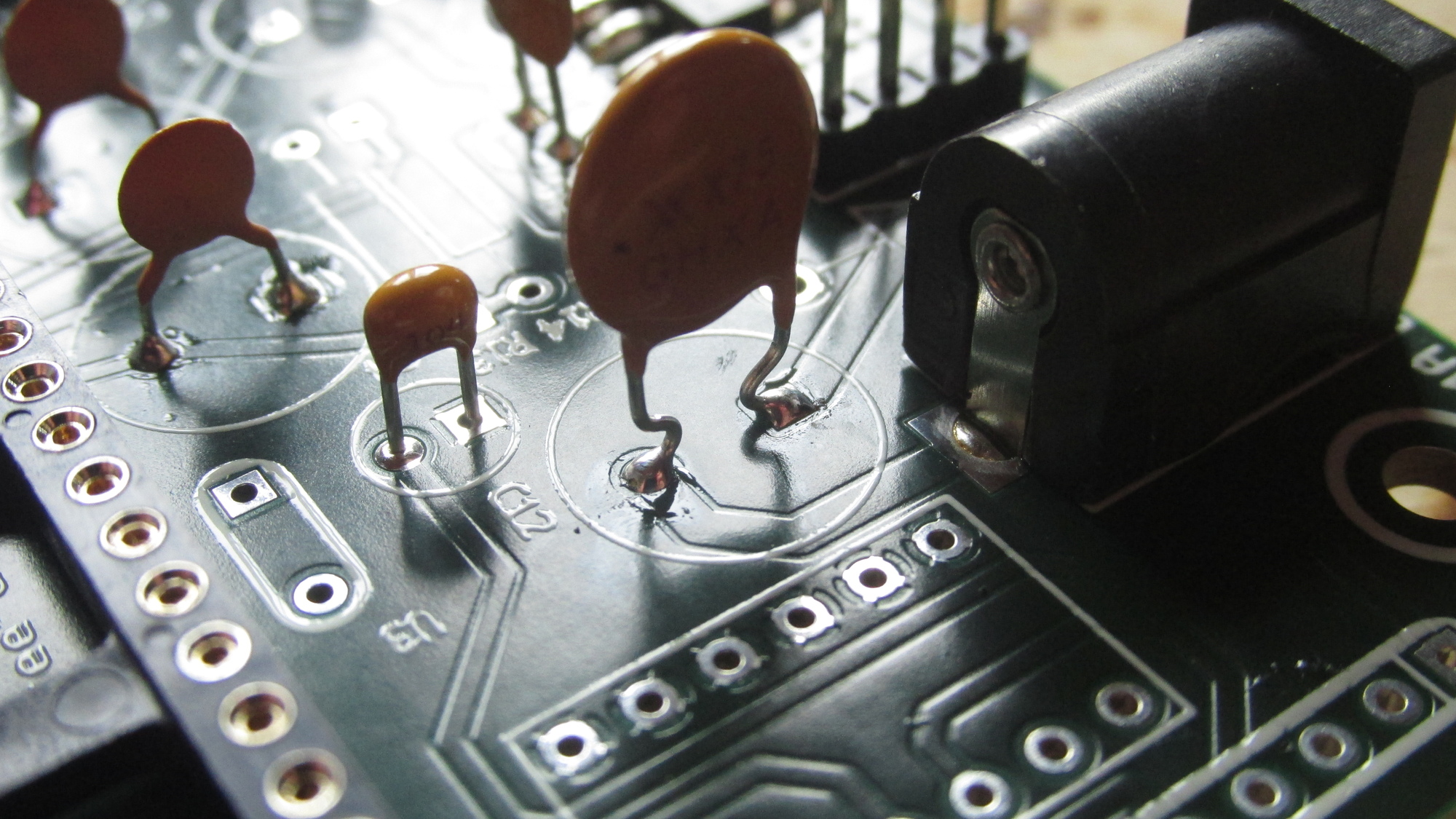
V1: Solder pins on both sides of PCB, cut leads
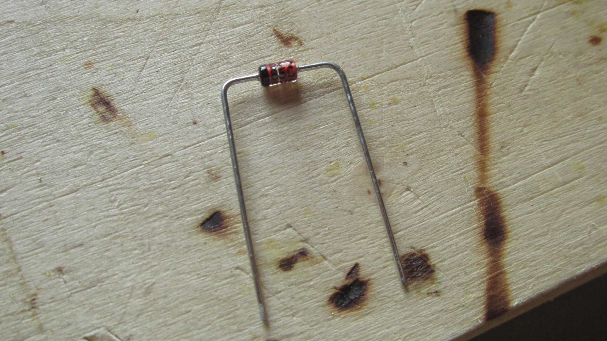
Z1: Prepare form factor, bent leads
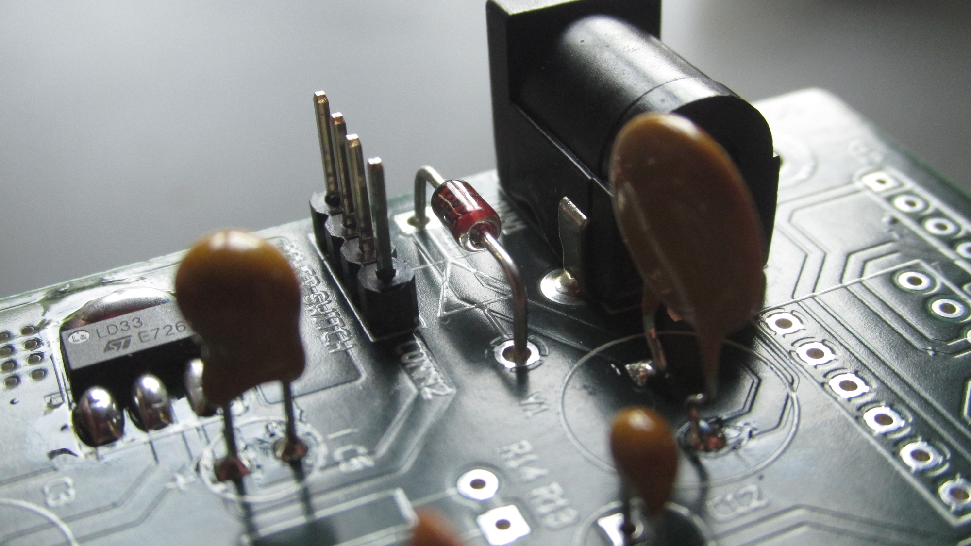
Z1: Place diode on PCB, bent leads on bottom side to make it remain in place
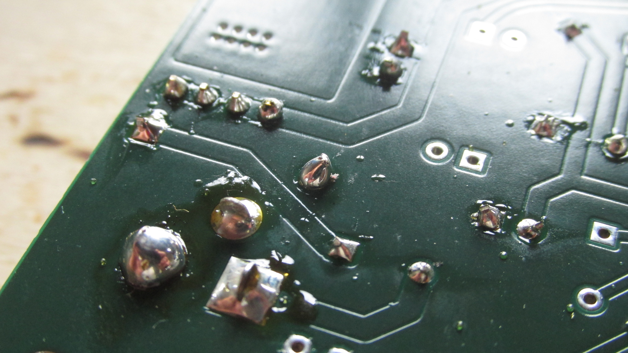
Z1: Solder pins, cut leads, apply heat again
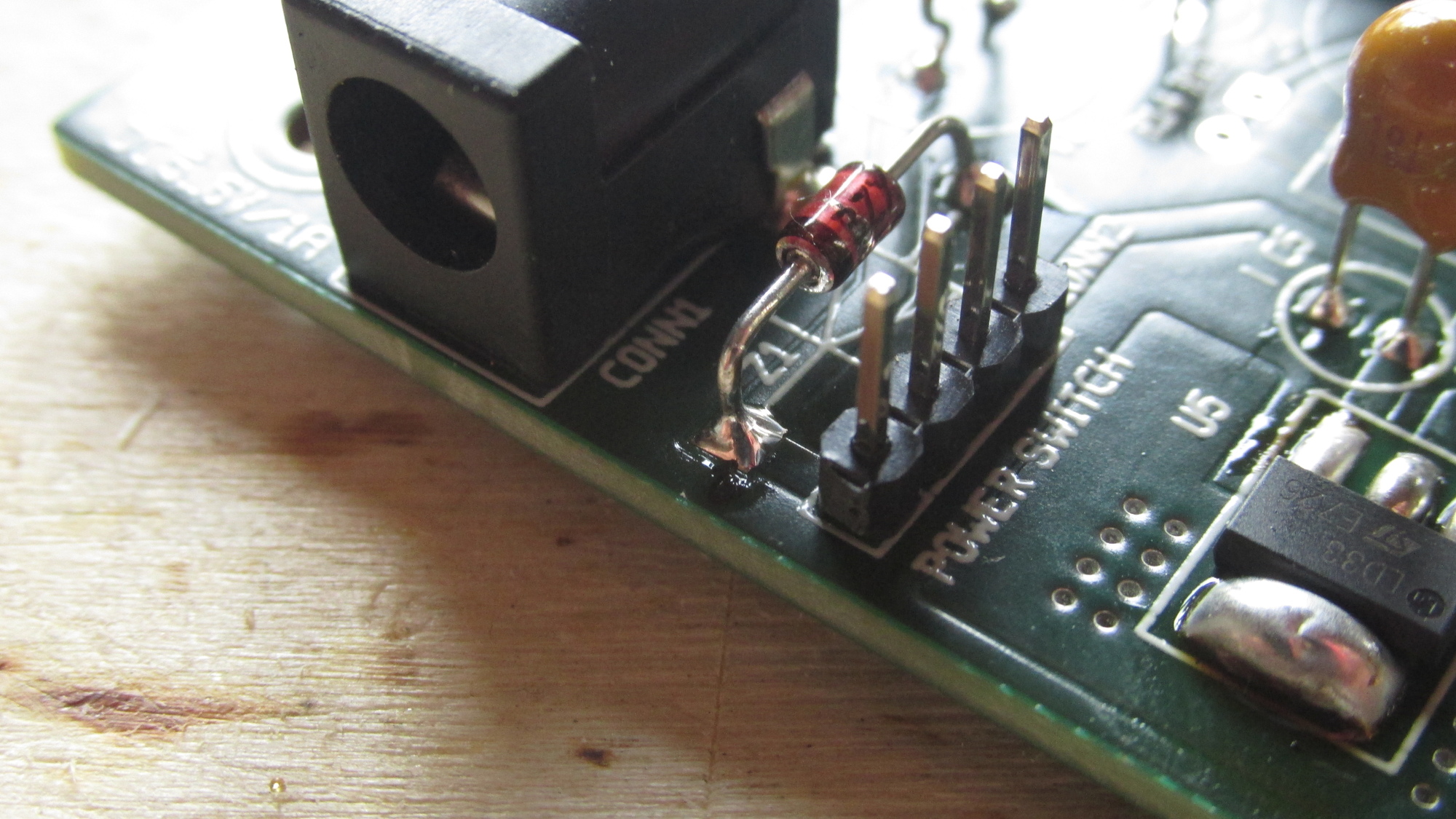
Z1: Fix solder on component side
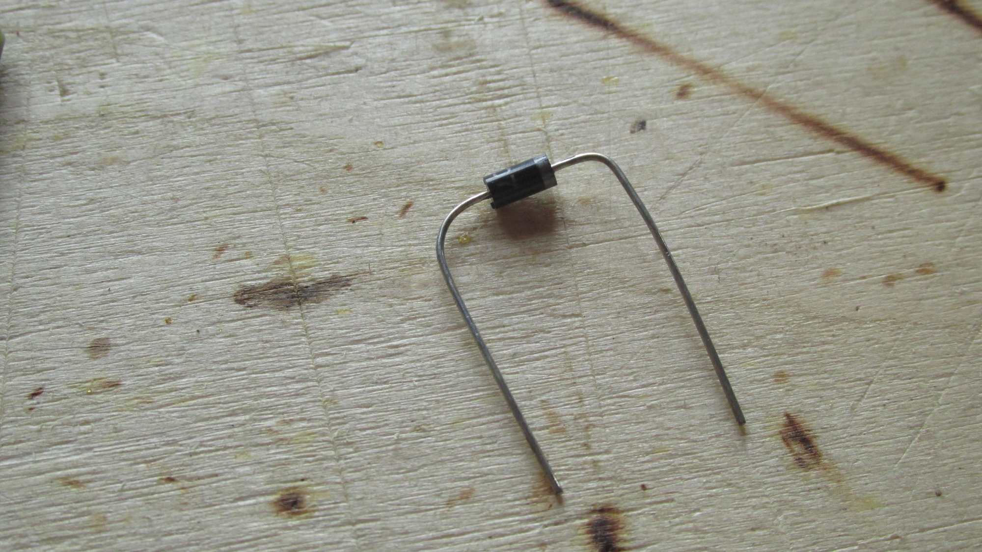
D8: Prepare form factor, bent leads
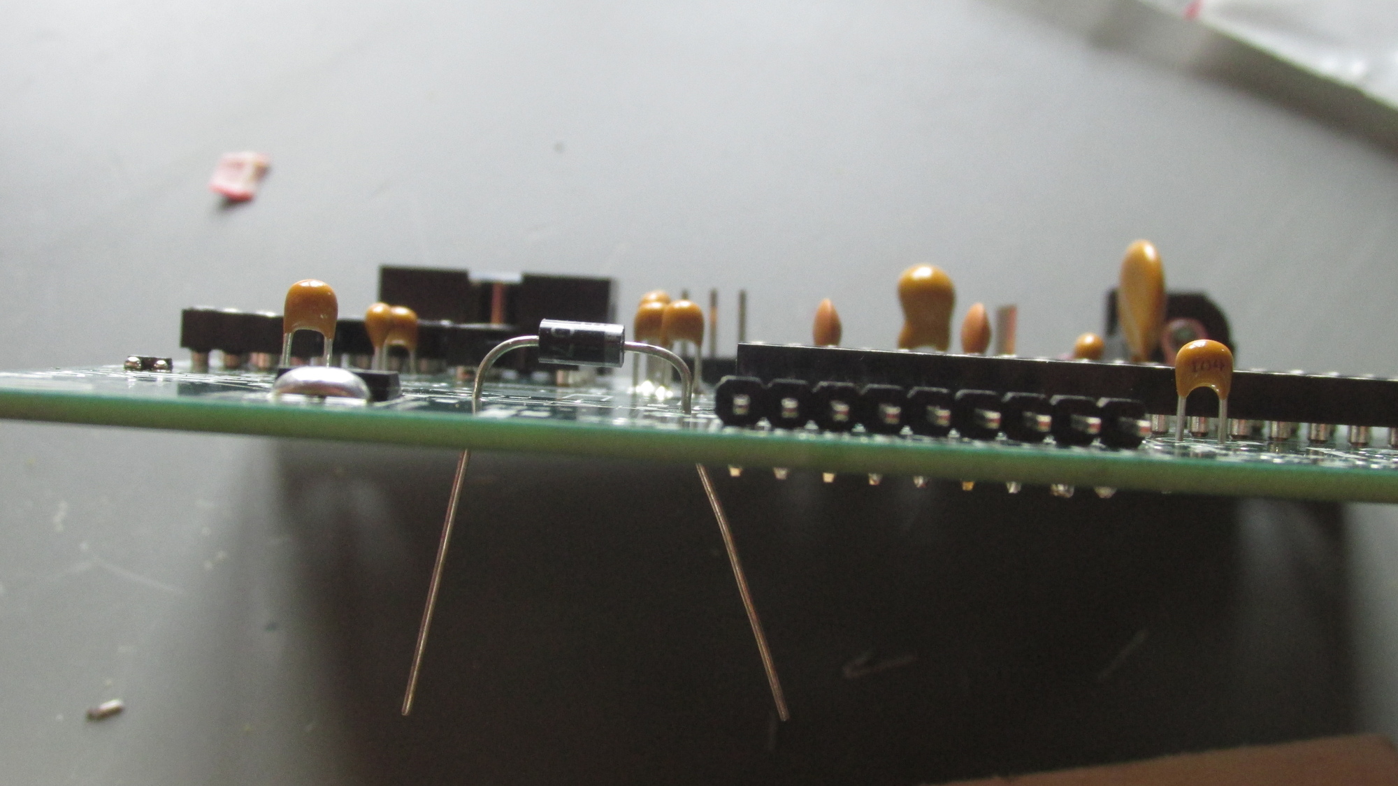
D8: Place diode on PCB, bent leads to make it remain in place, solder pins
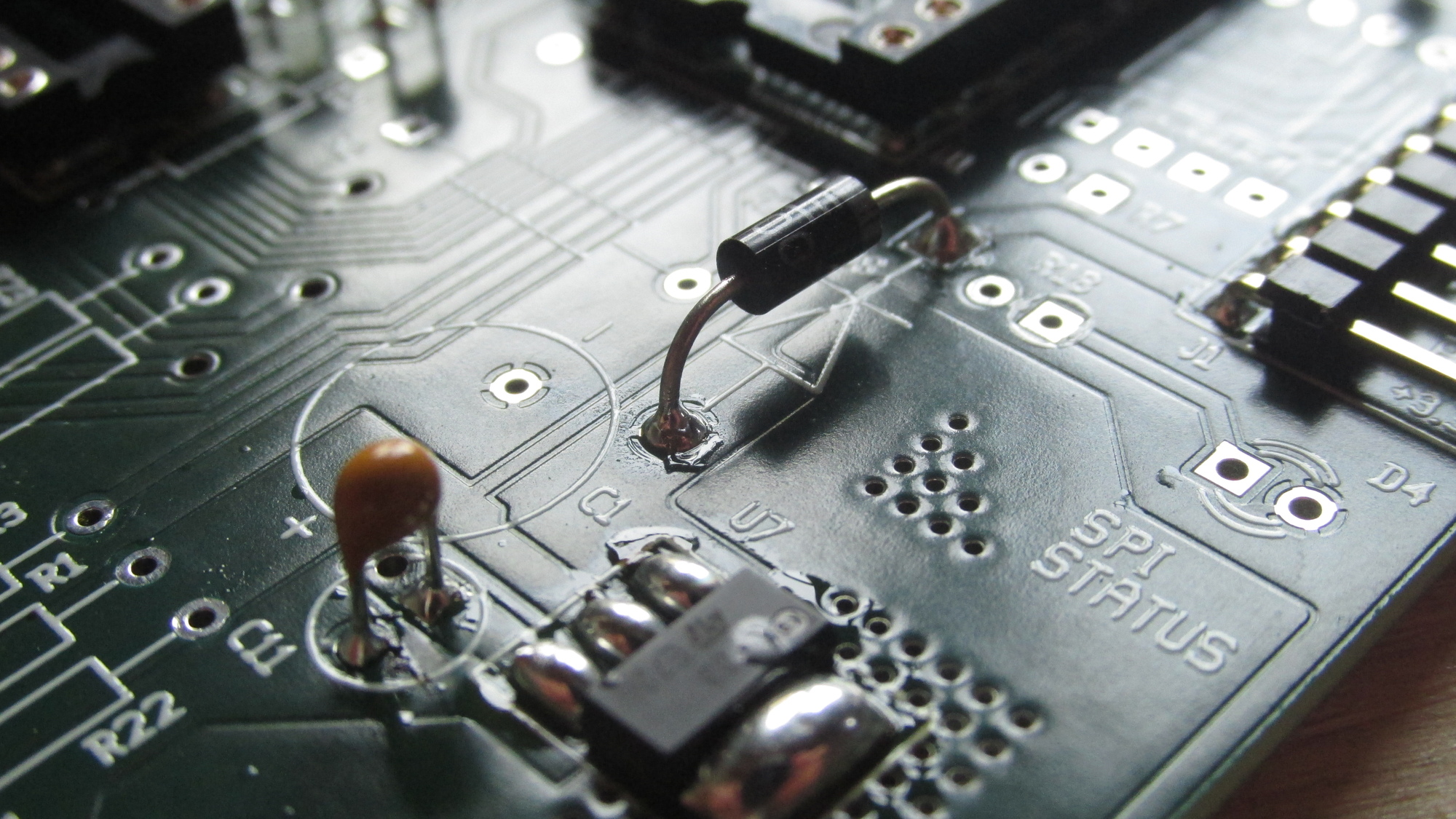
D8: Fix solder on component side, if required
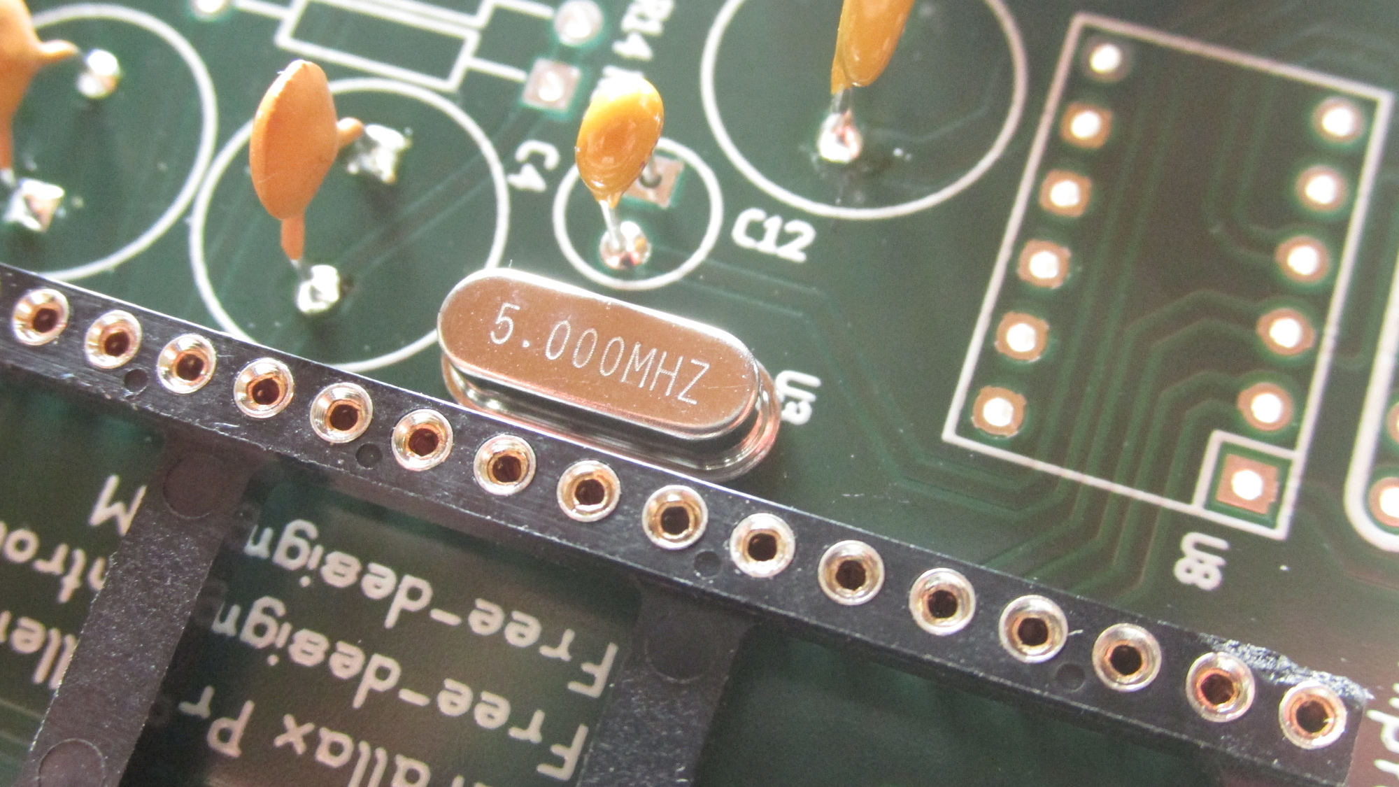
U3: Place component on PCB
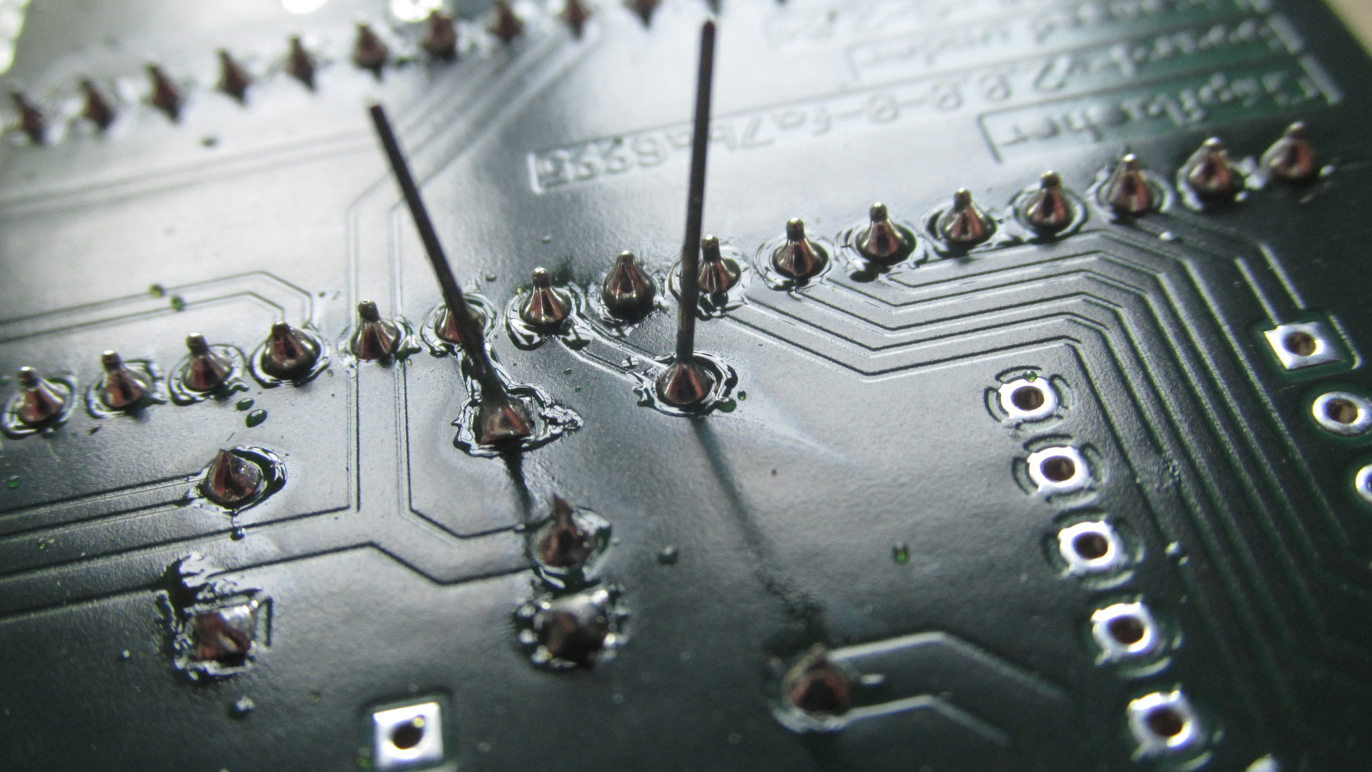
U3: Slightly bent leads to make component remain in place, solder pins, cut leads
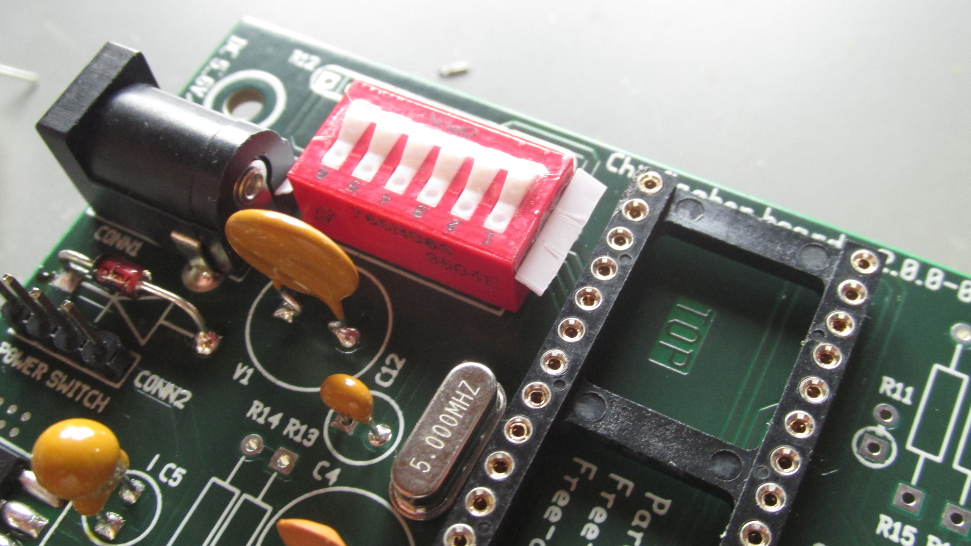
U8: Place component on PCB
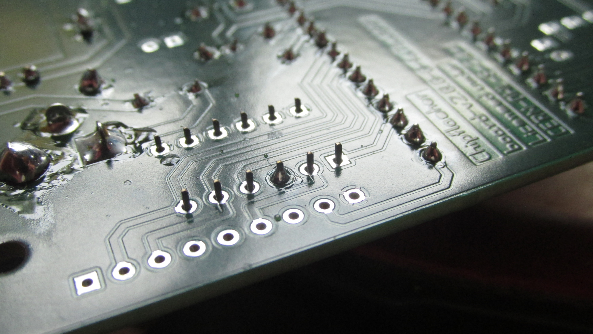
U8: Solder one center pin, check for flat position on PCB
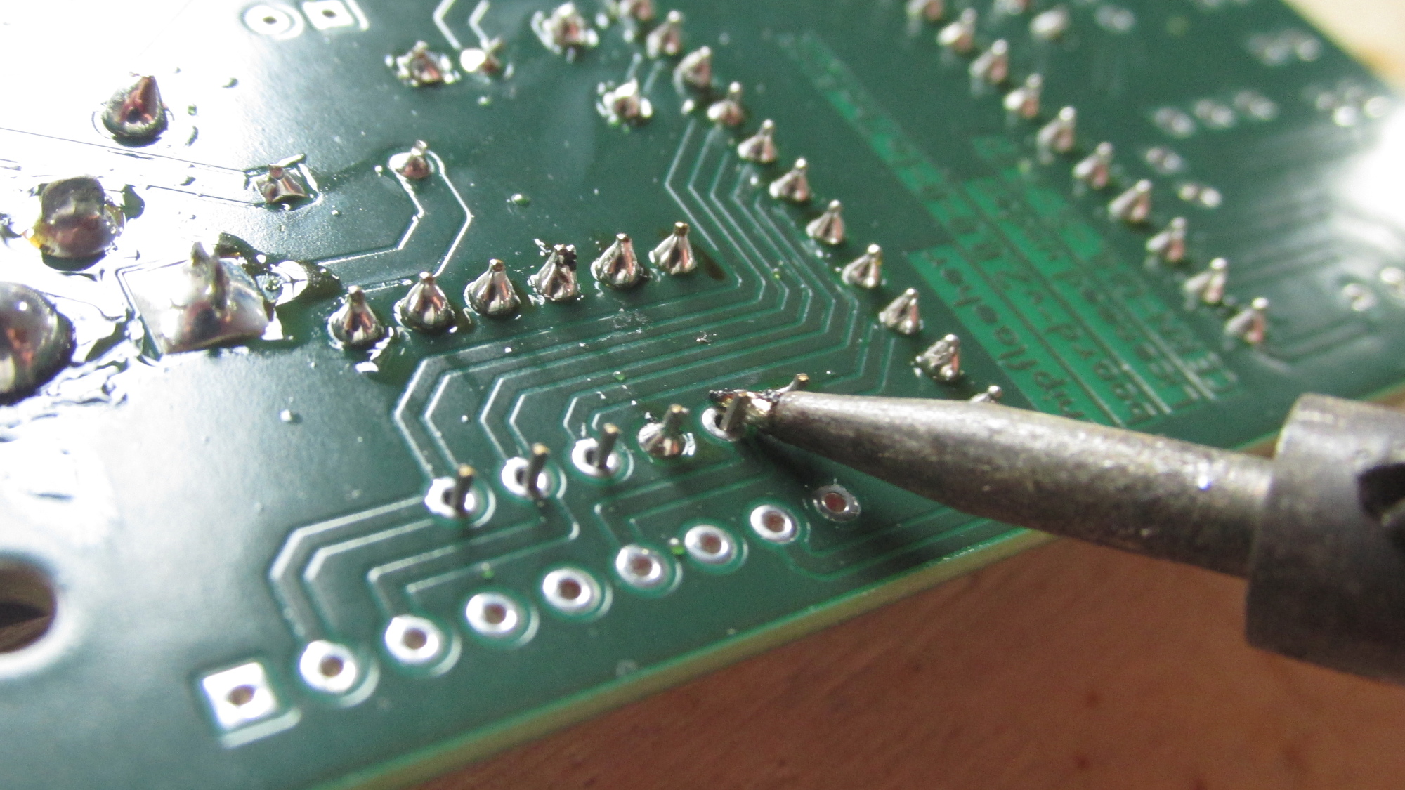
U8: Solder remaining pins, thermals will heat up like 5 times slower!
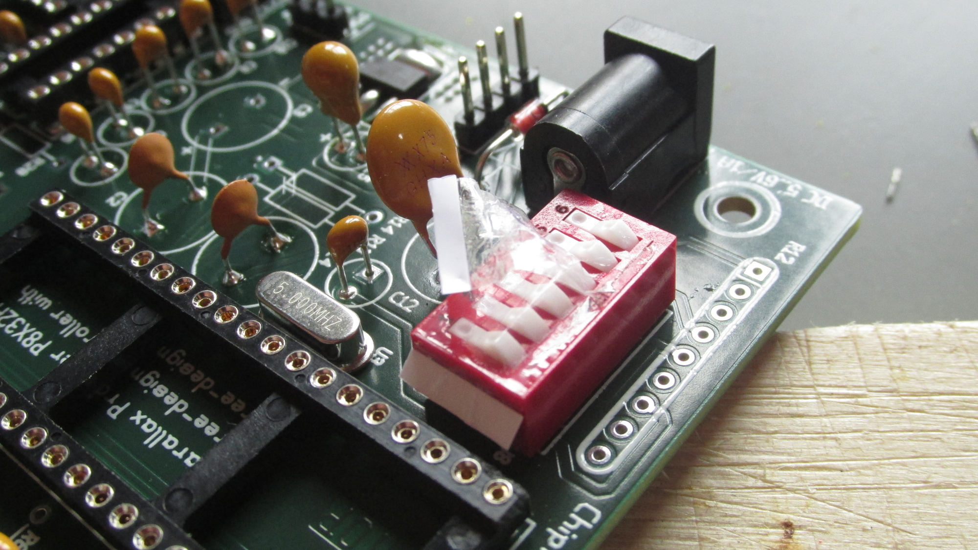
U8: Remove protective foil
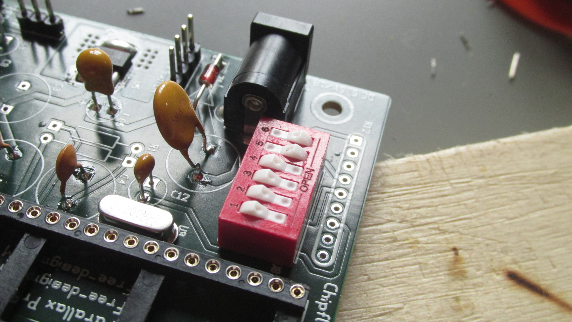
U8: Clean-up, check mechanical function of switches
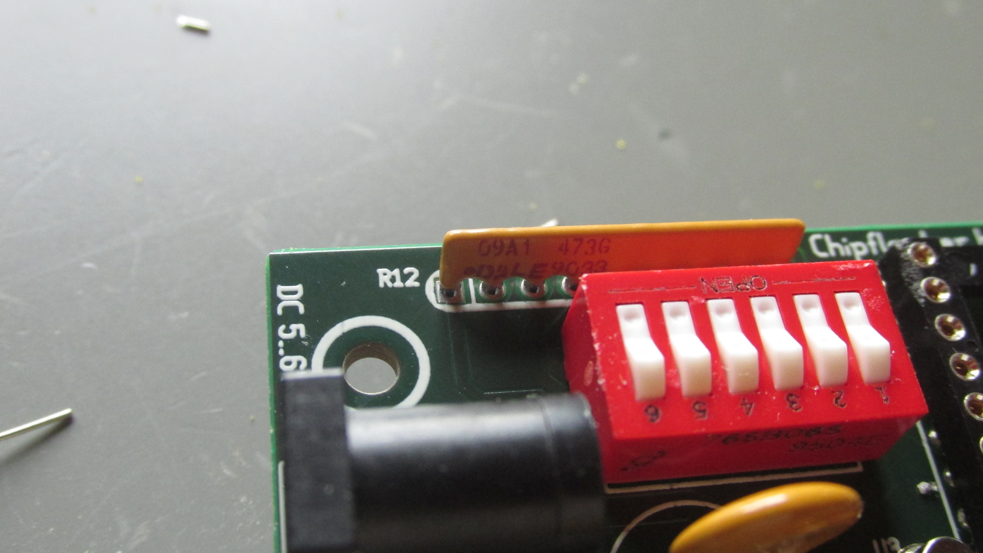
R12: Place component on PCB, align dotted pin to square pad
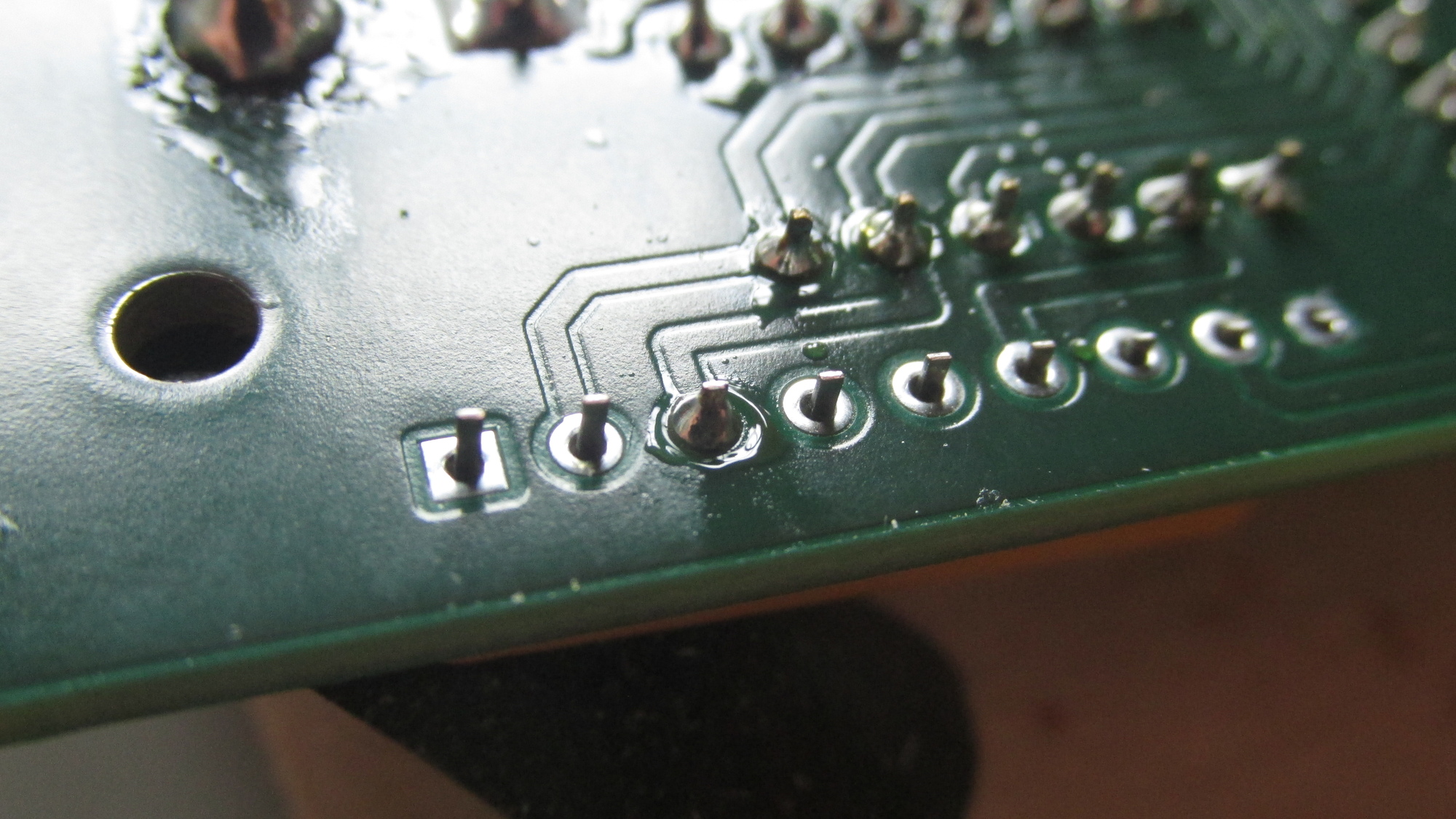
R12: Solder one pin
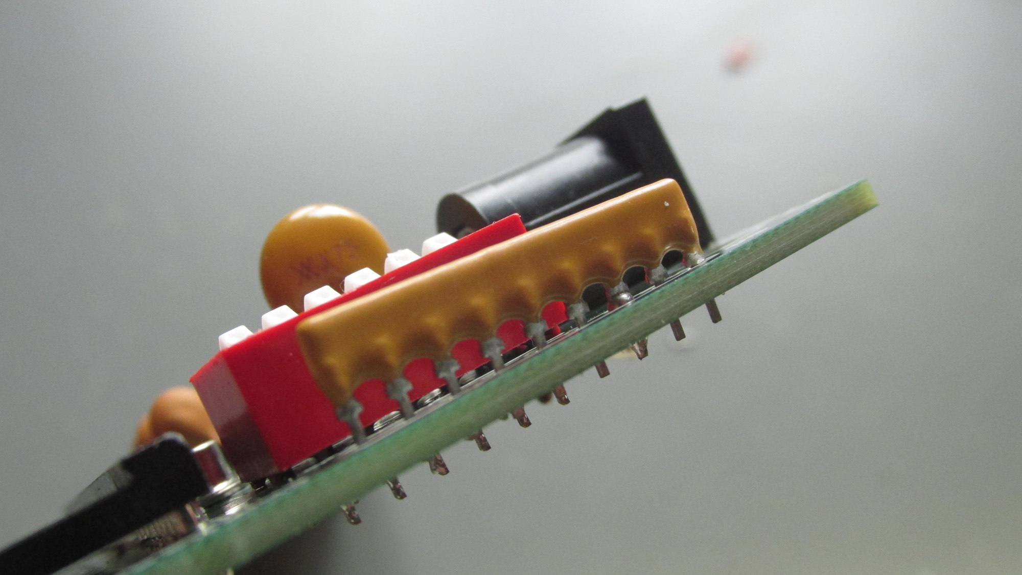
R12: Check for flat position on PCB
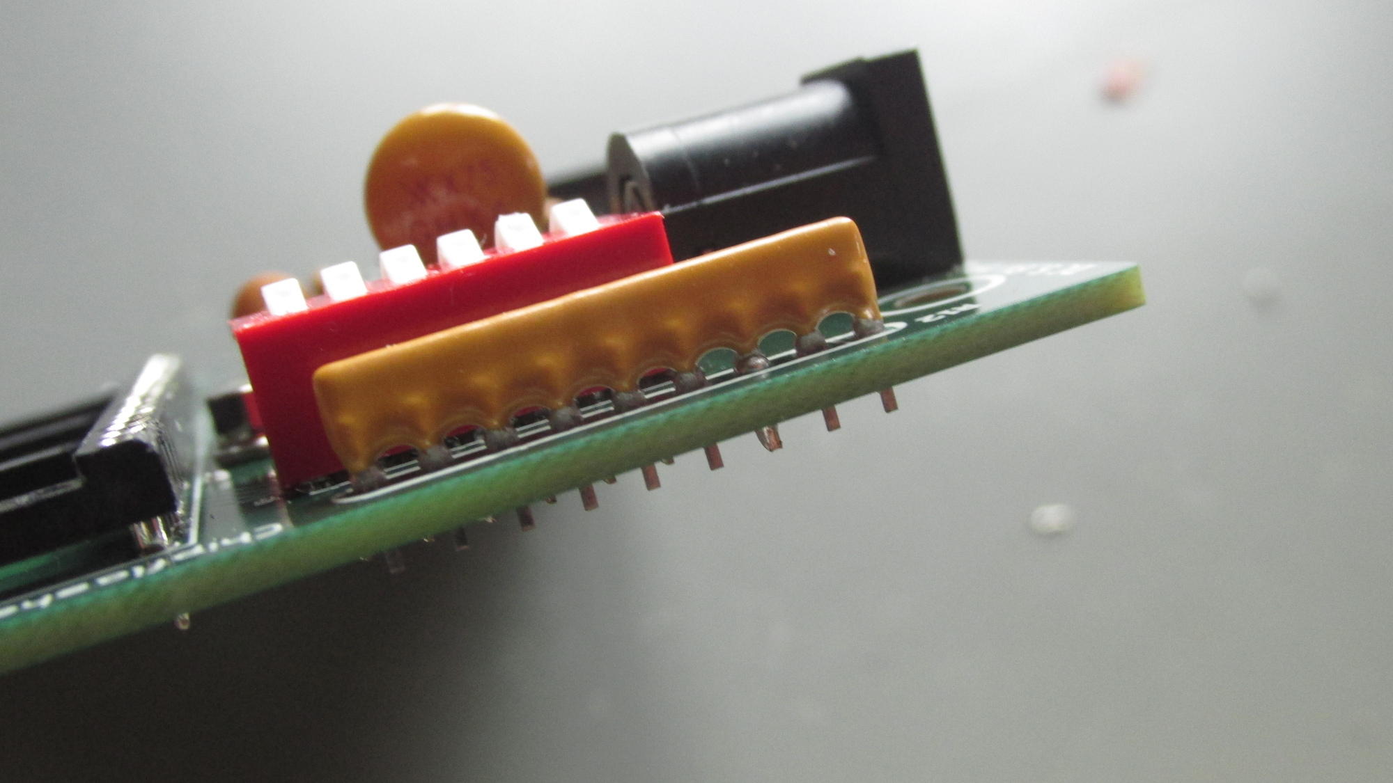
R12: Apply heat, fix position
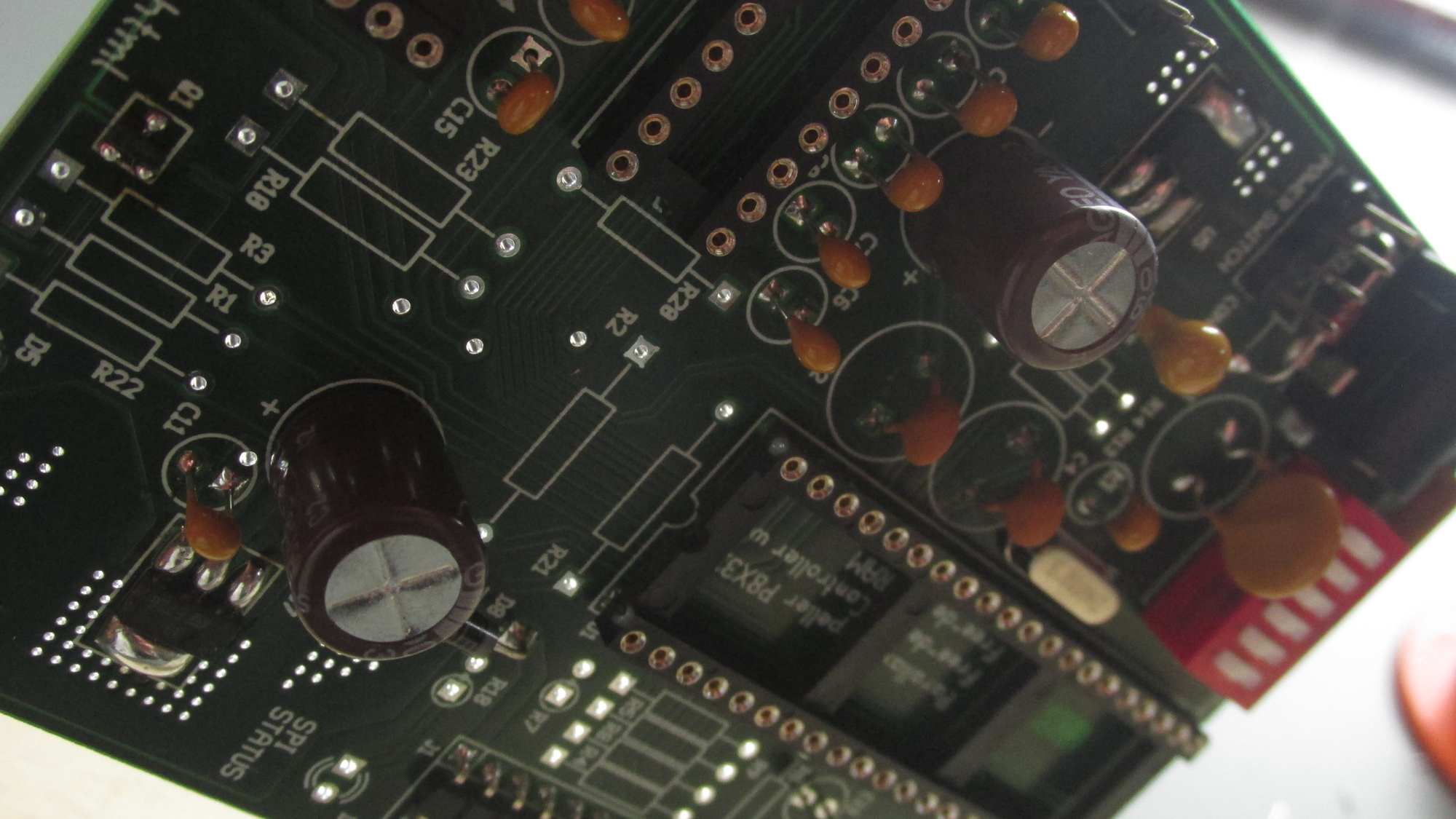
C1, C3: Flip PCB 90°, place capacitors on PCB

C1, C3: Solder pins, cut leads, apply heat again to make solder look nice
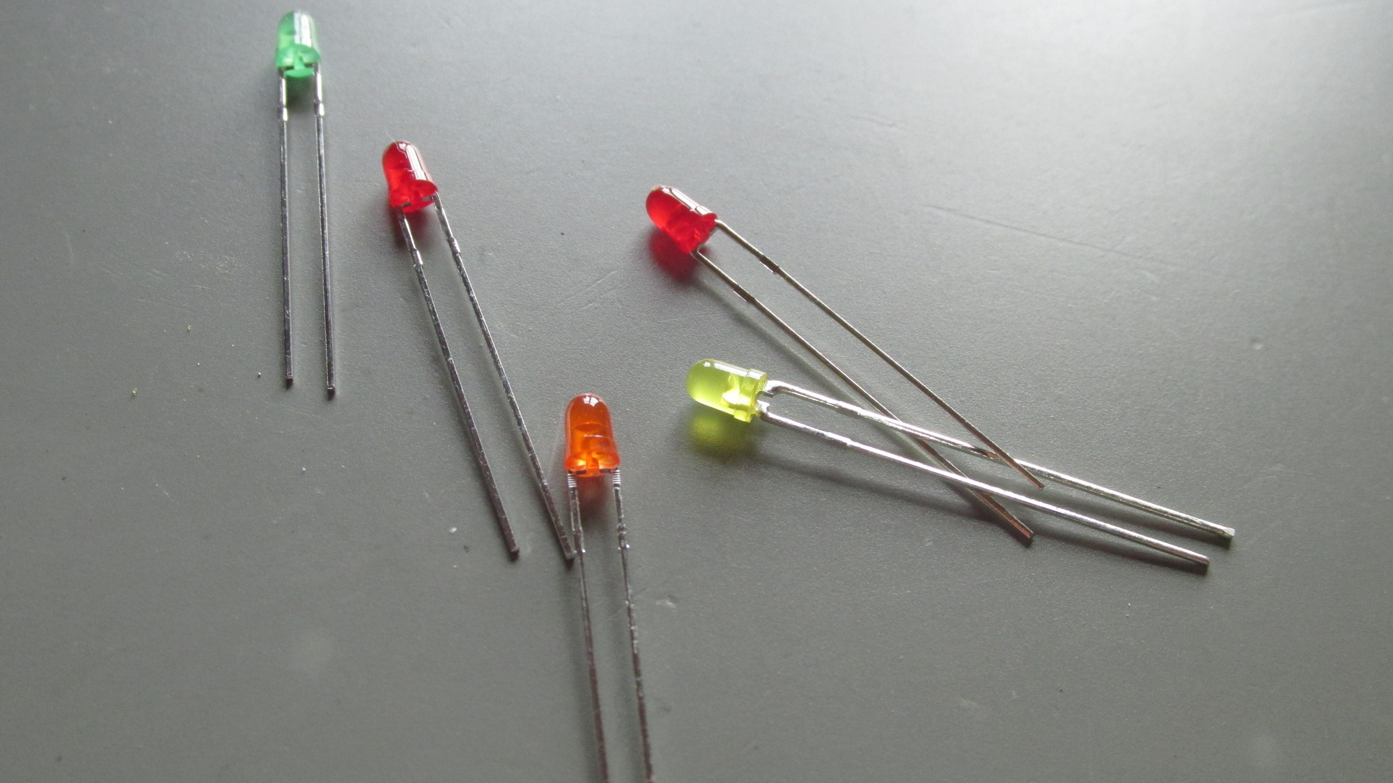
D1, D2, D3, D4, D5: Collect components
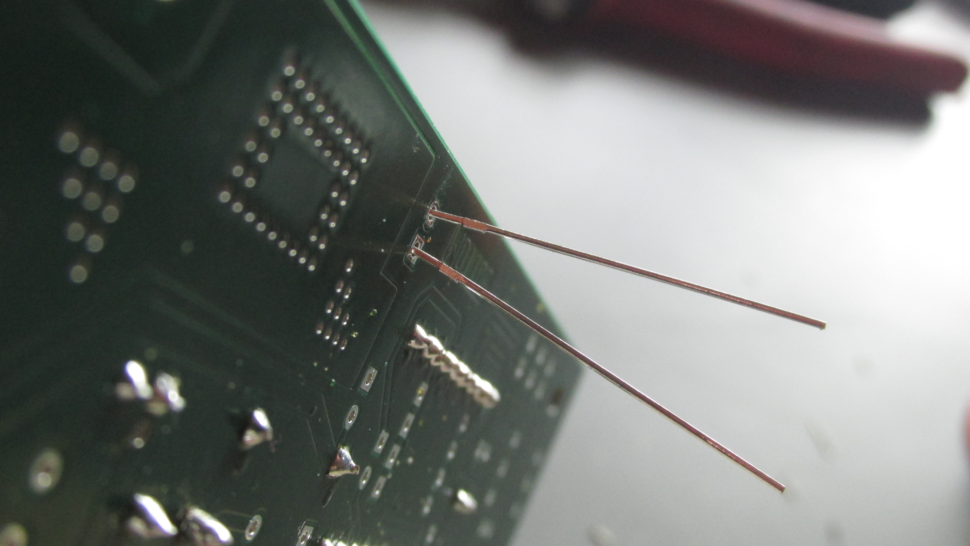
D1, D2, D3, D4, D5: Place components on PCB, spread leads slightly, make sure that longer lead will contact squared pad!
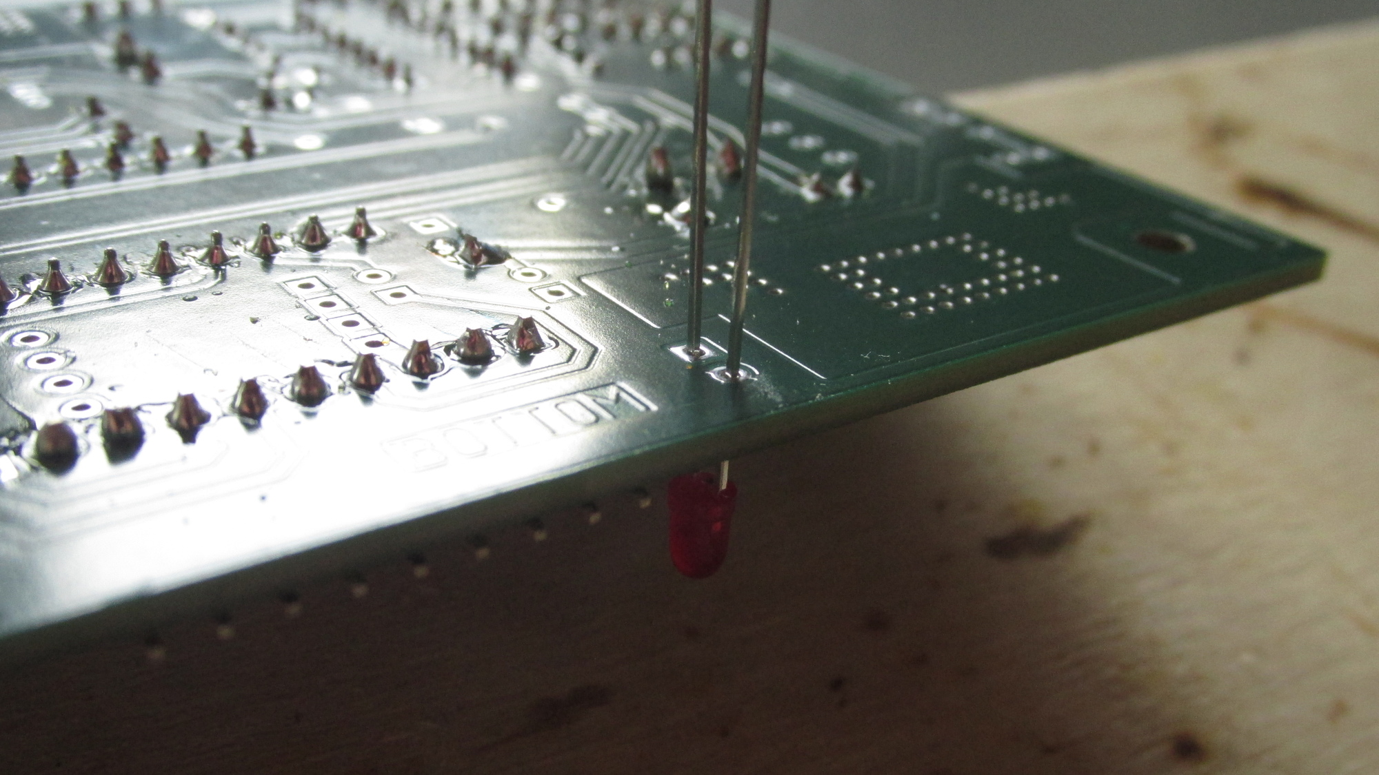
D1, D2, D3, D4, D5: Pull LEDs until flat lead markings disappear on bottom side
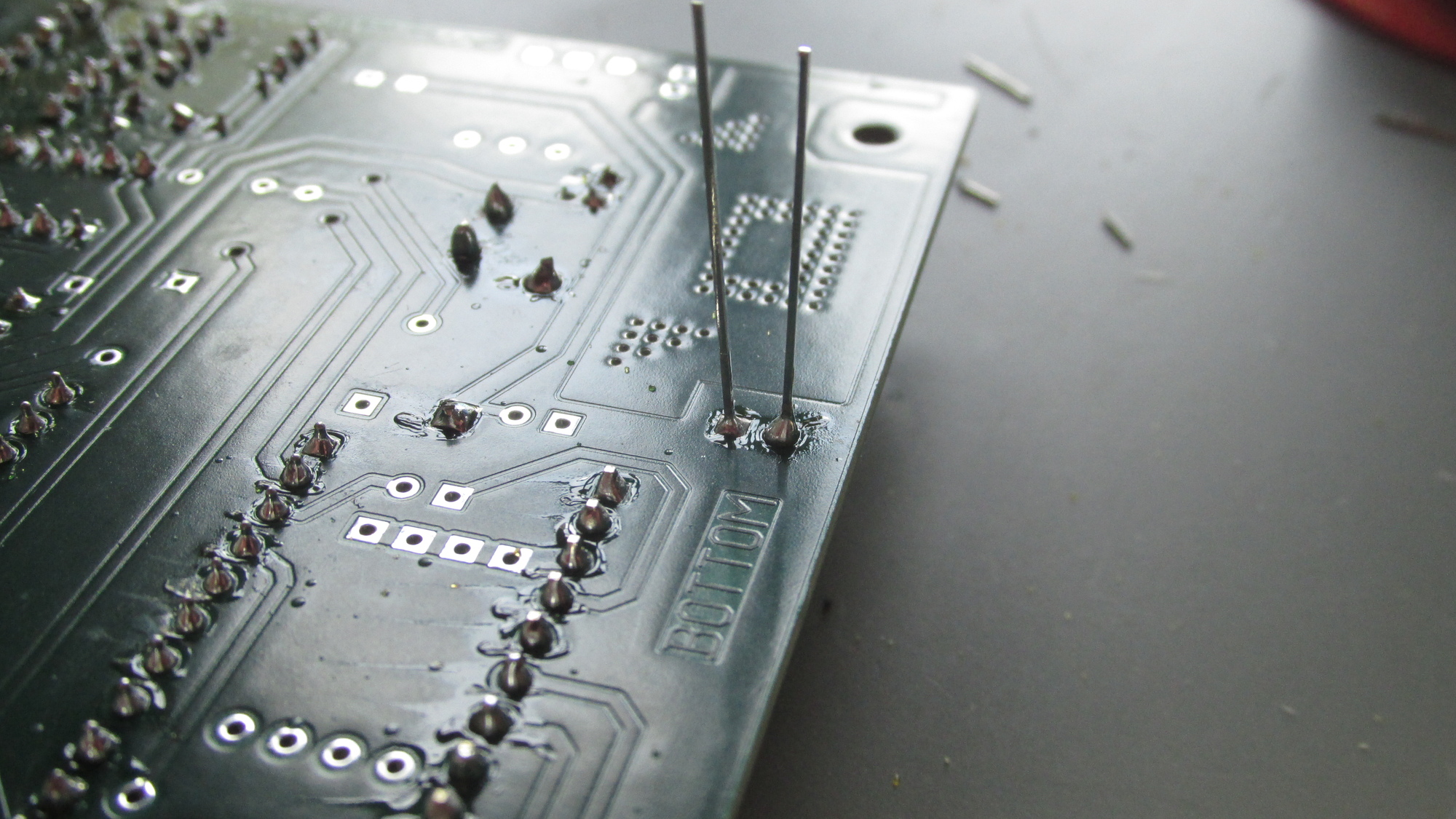
D1, D2, D3, D4, D5: Solder pins, apply heat as short as possible!
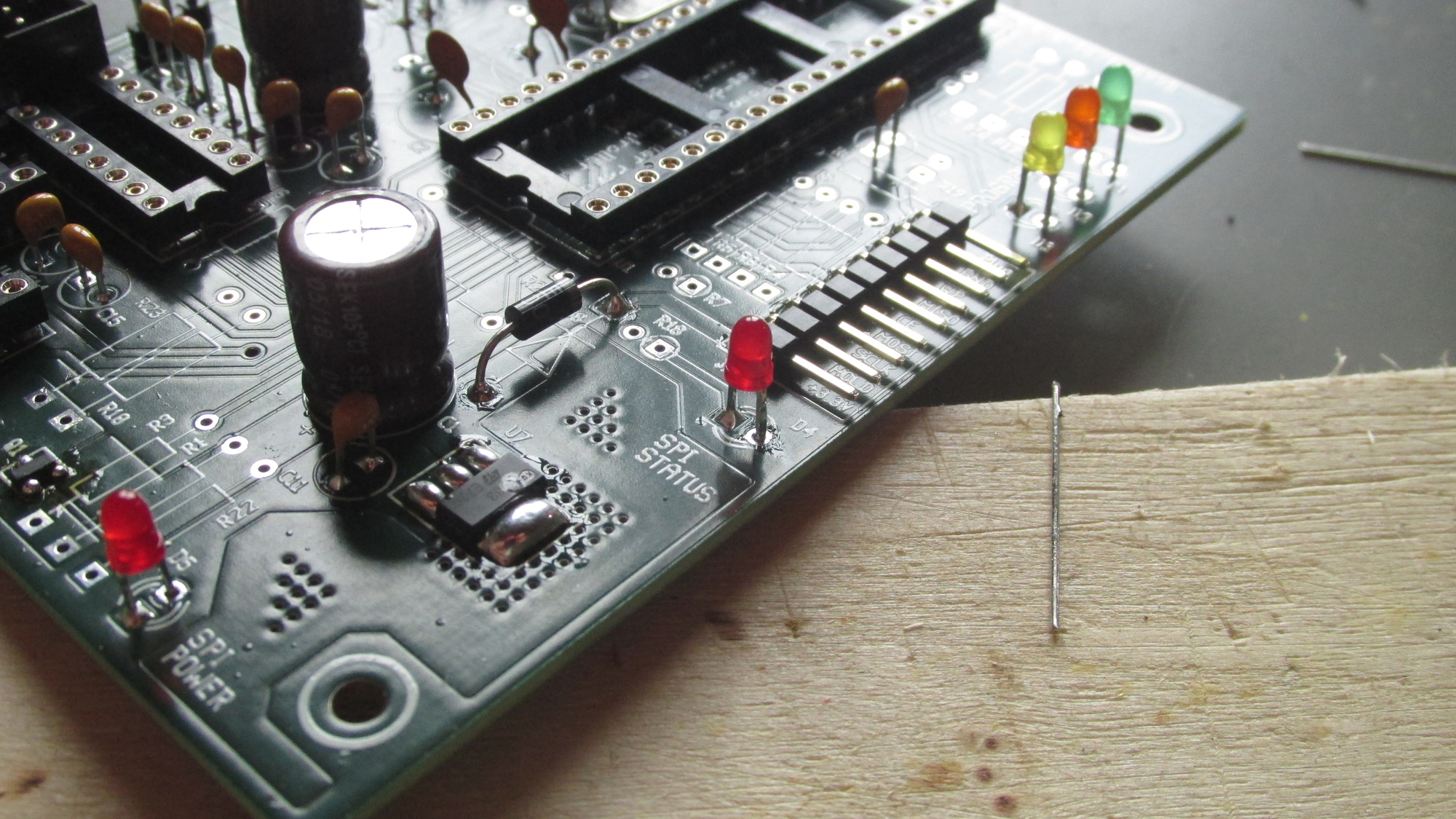
D1, D2, D3, D4, D5: Do not try to apply solder on component side, additional heat will break LEDs!
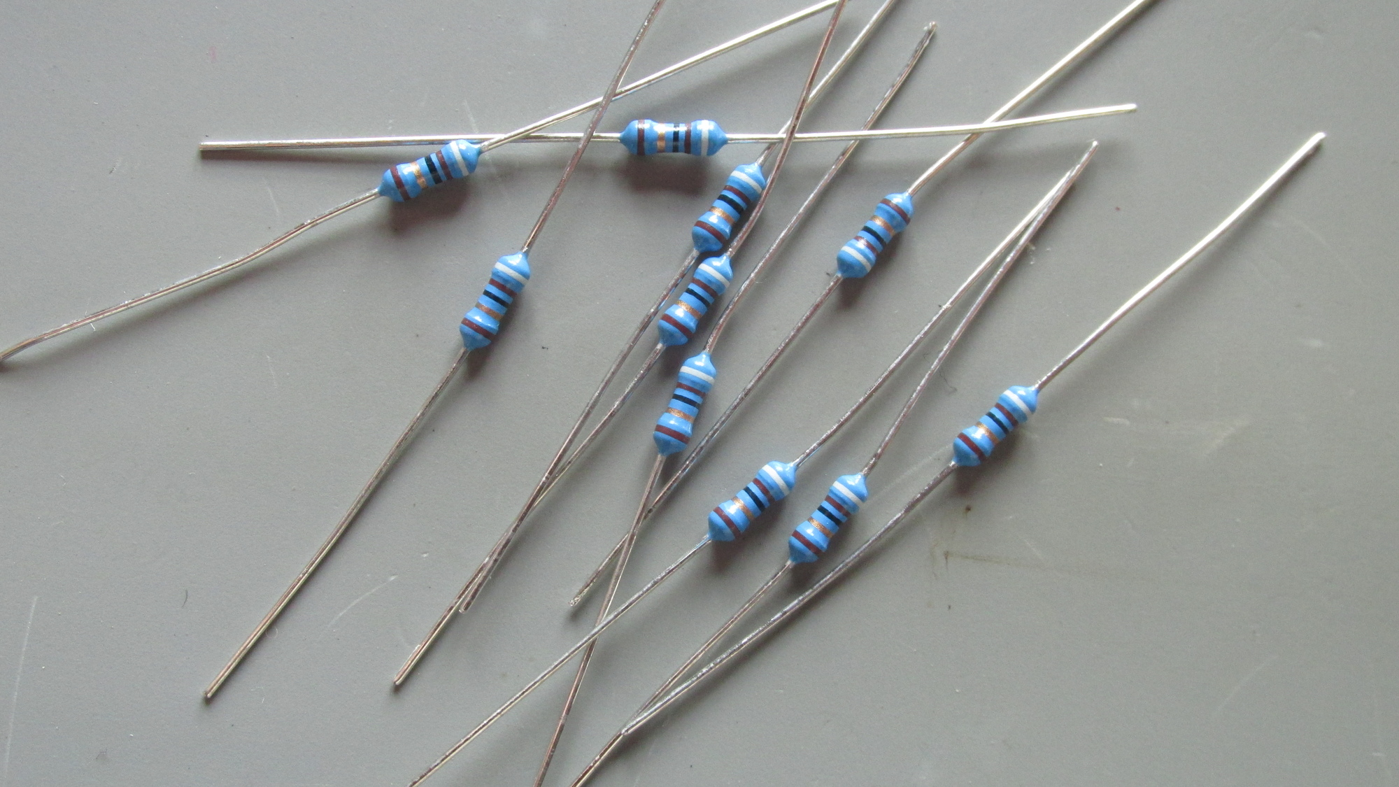
R3..R11, R23: Collect components, check color code
Please notice that R10 and R23 have been changed in 2025:
R10 should be set 100Ohm, R23 to 1000Ohm. These resistors are wired in parallel, forming the pull-up resistor for the CEn line of SPI. It turned out that the initial value for R_pull of just 45.5Ohm (R10 and R23 set to 91Ohm) is too small and will make the chip probe action fail, very likely. In addition, PCBs should provide sockets for these resistors. In case other use cases require different values, both resistors could be changed easily.
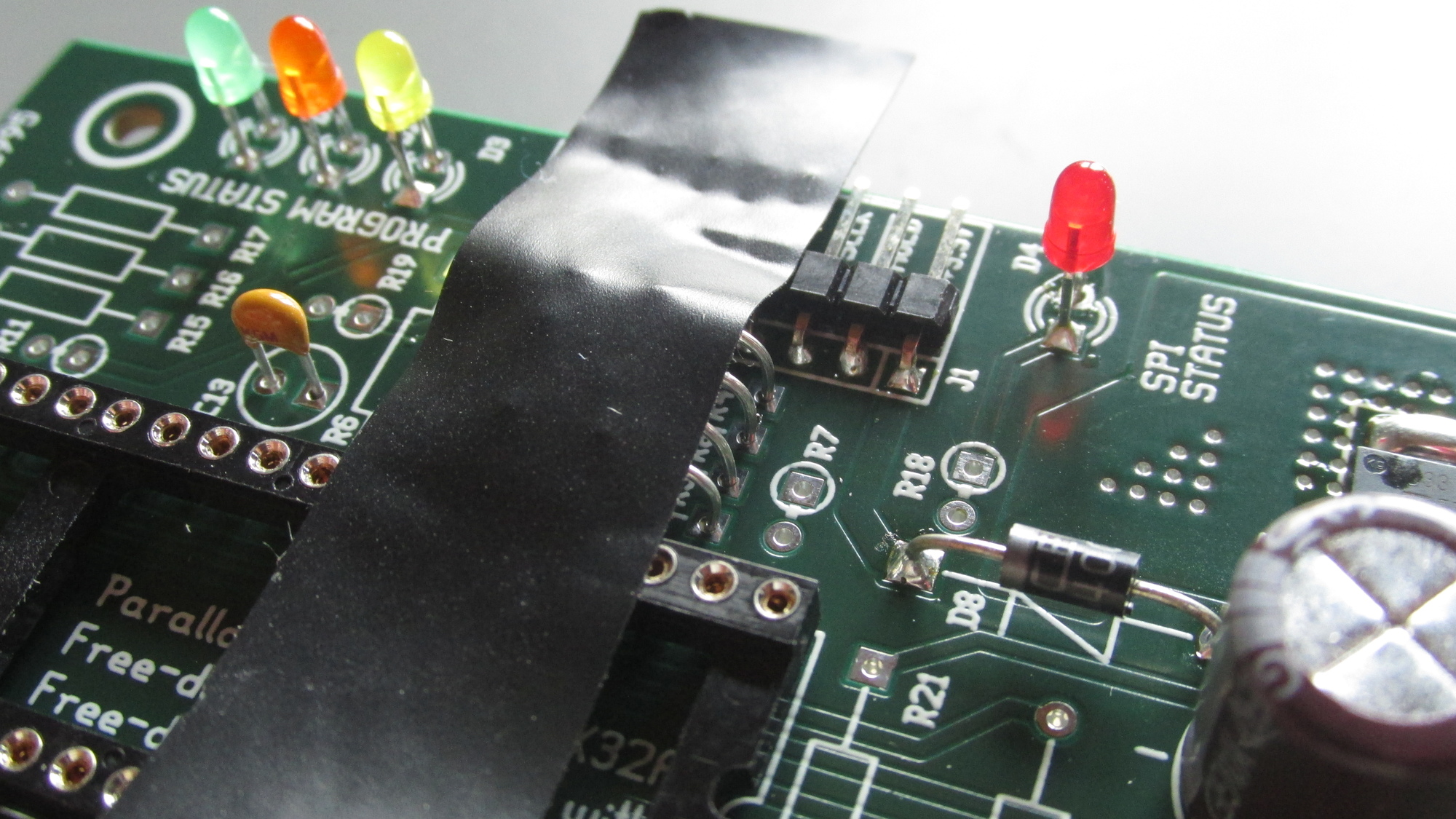
R4, R5, R8, R9: Place components on PCB, fix with tape
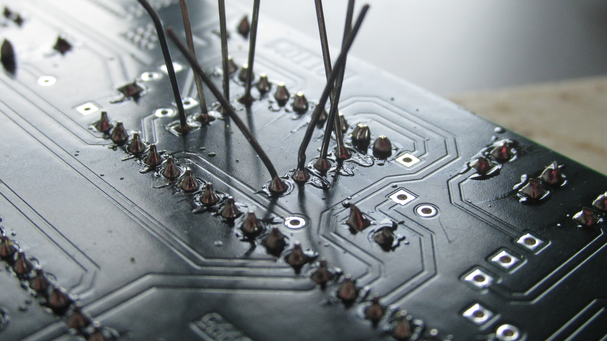
R4, R5, R8, R9: Apply solder on bottom side
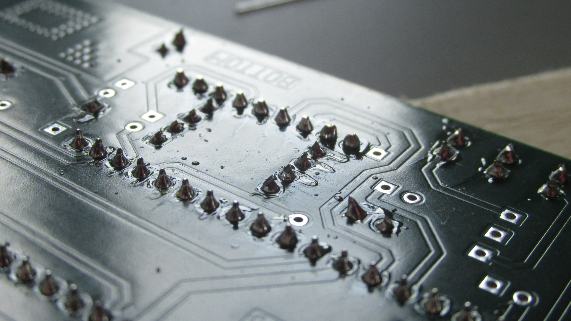
R4, R5, R8, R9: Cut leads
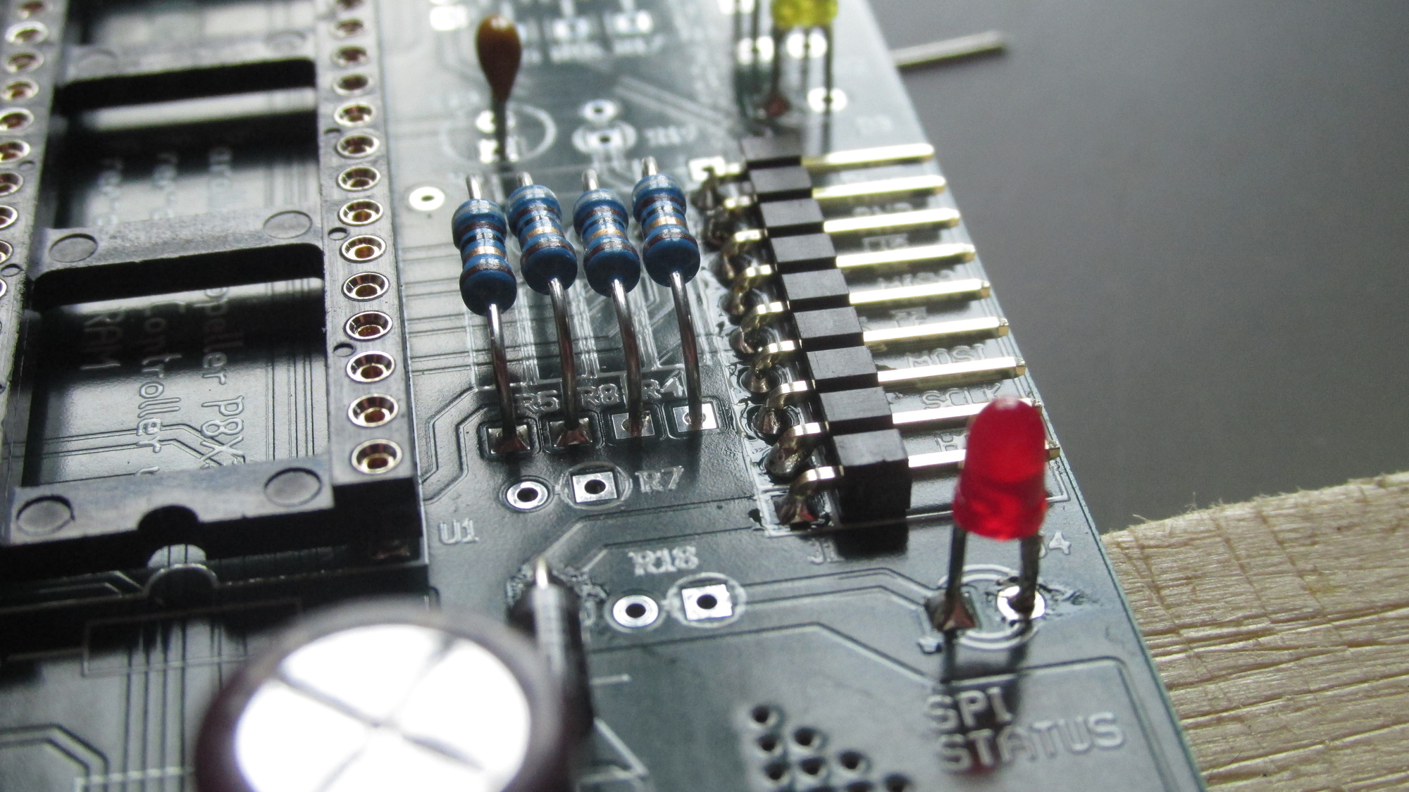
R4, R5, R8, R9: Check solder on component side
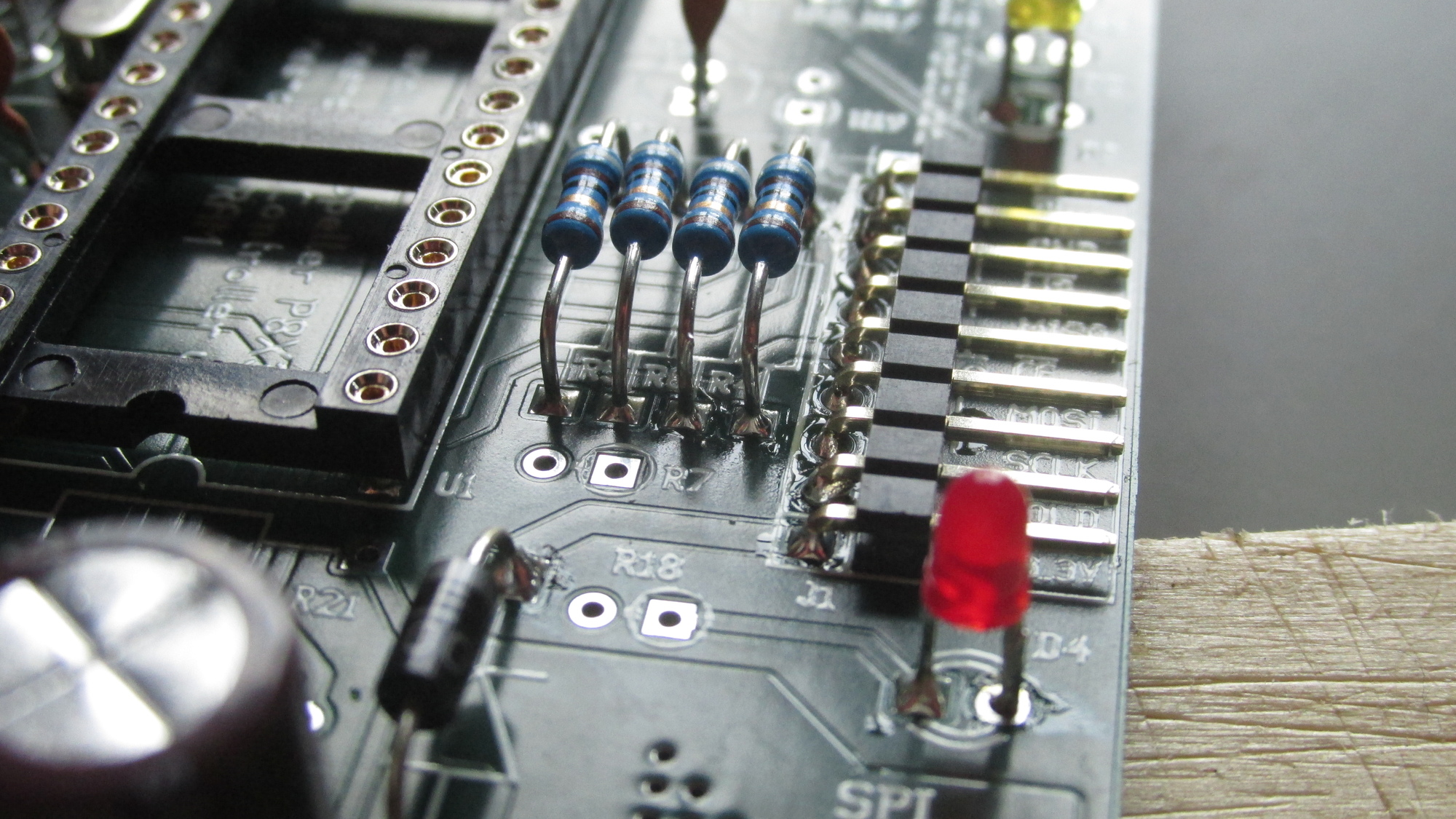
R4, R5, R8, R9: Add solder on component side if missing
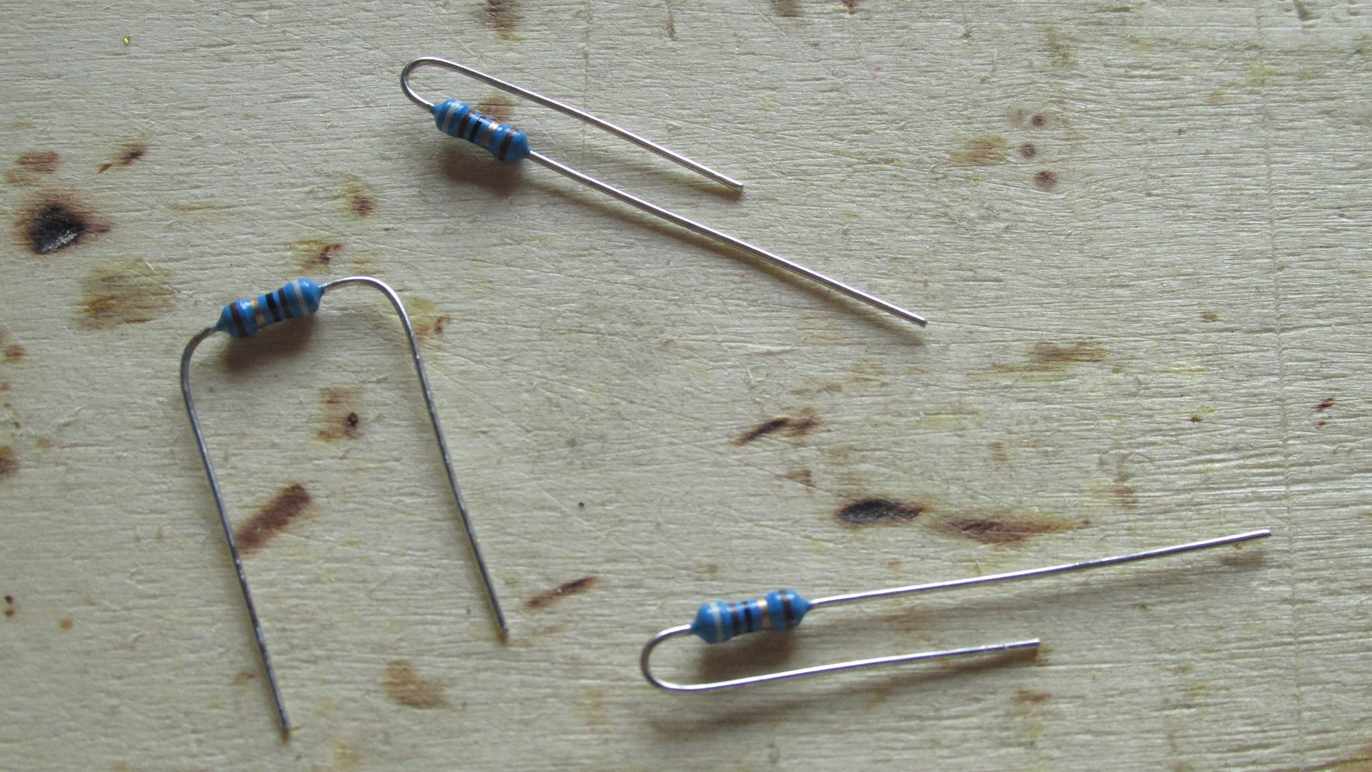
R6, R7, R11: Adjust form factor
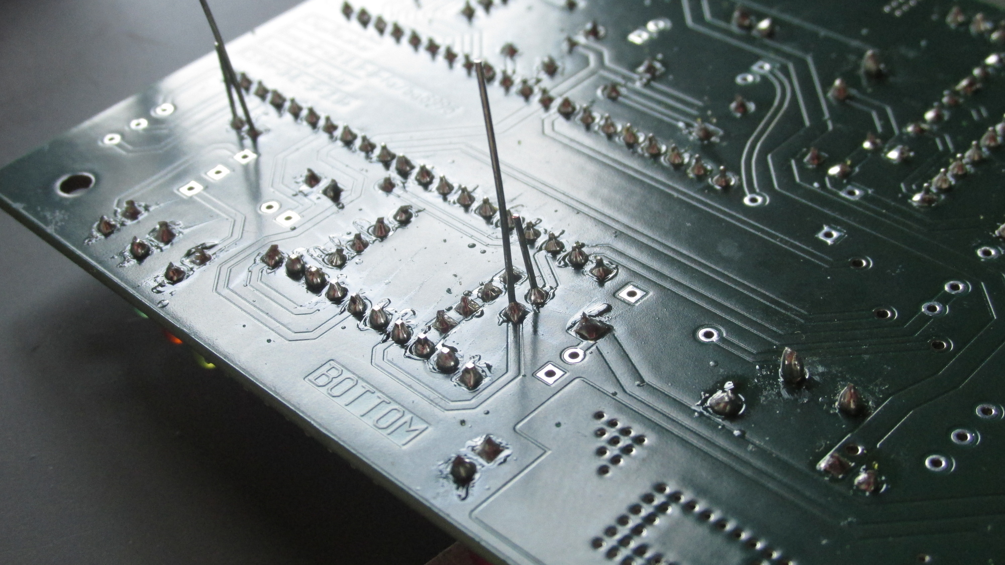
R6, R7, R11: Place on PCB, add solder on bottom side
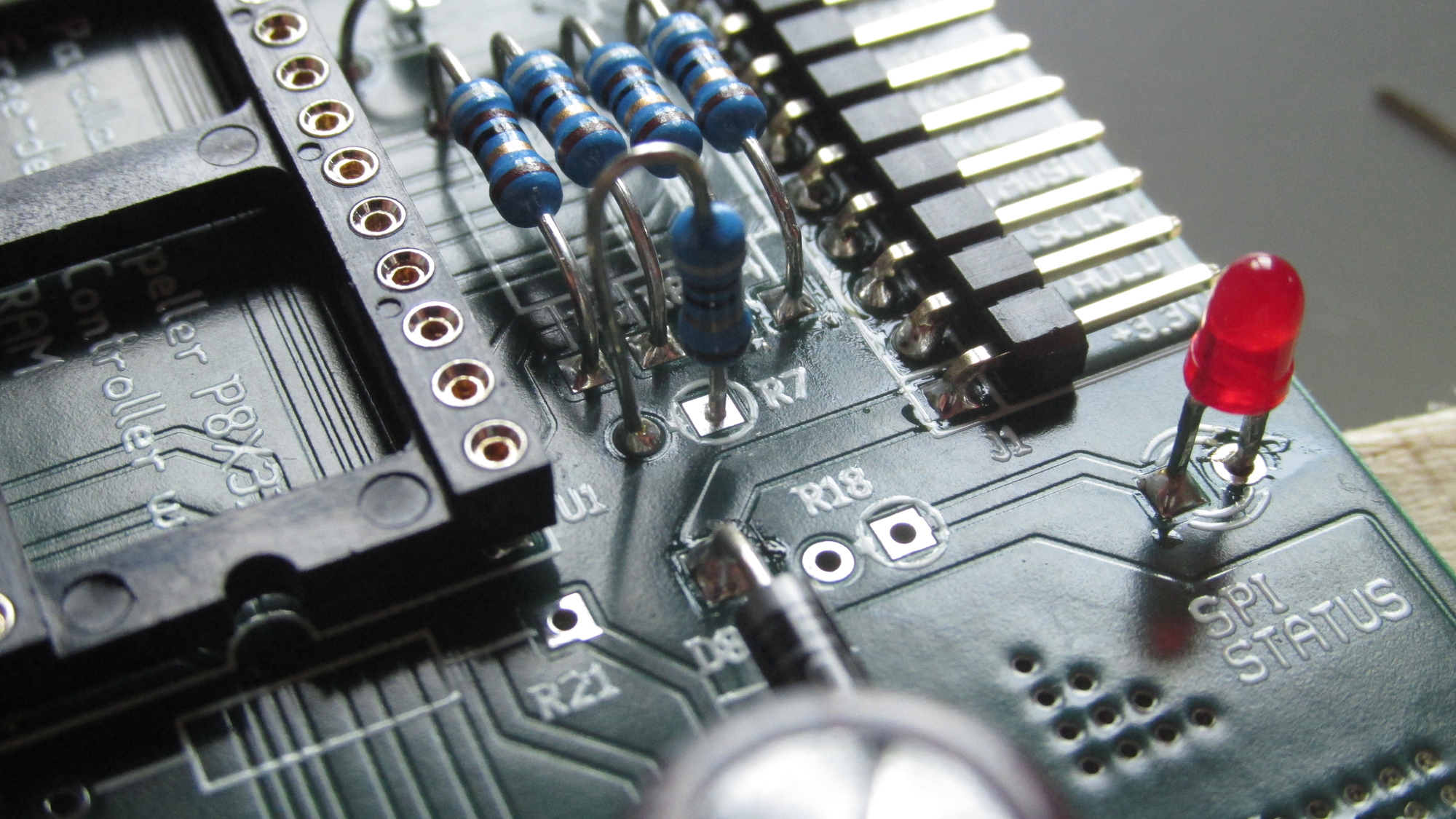
R6, R7, R11: Check pad on component side
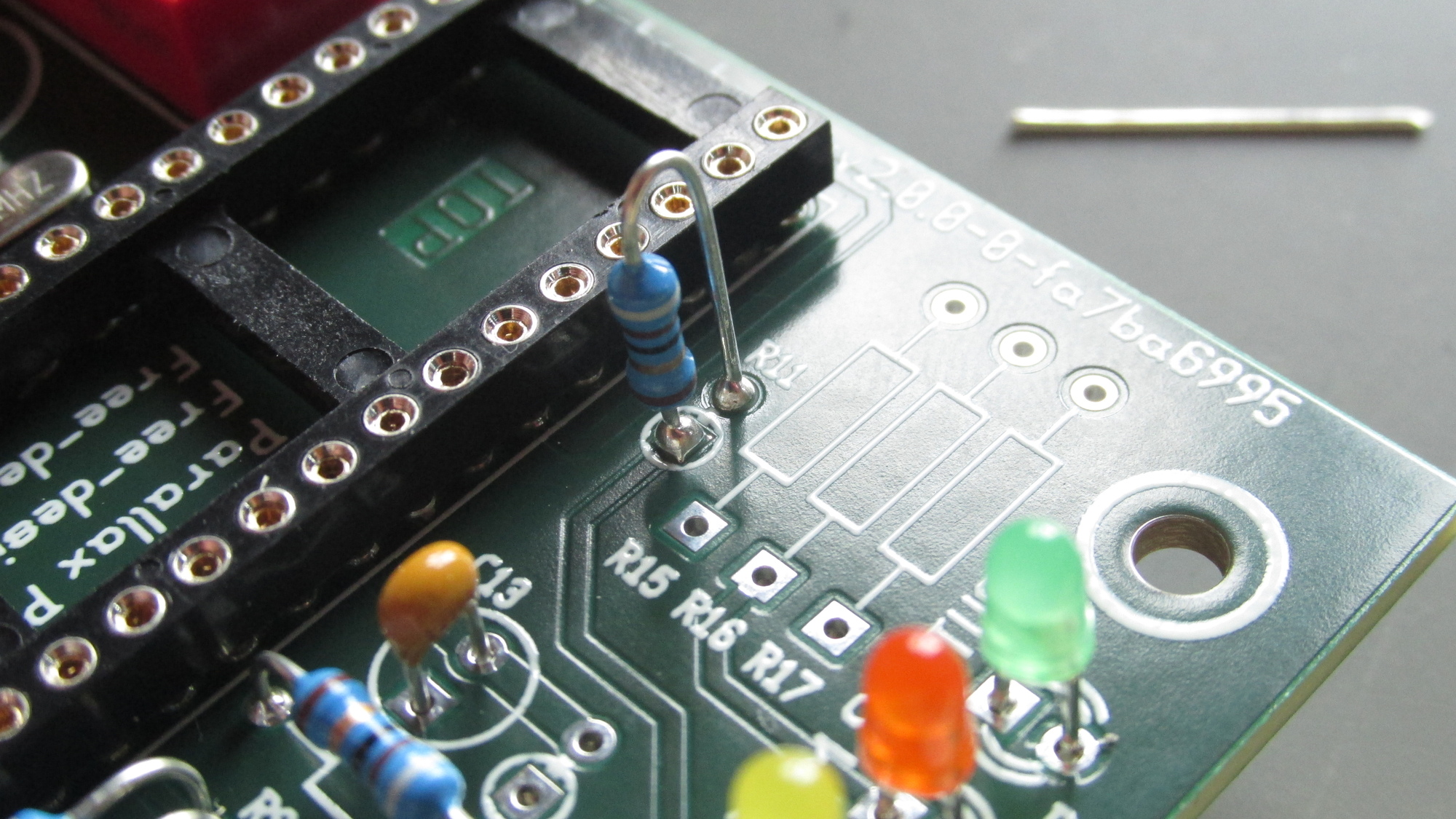
R6, R7, R11: Add solder on top side, if missing
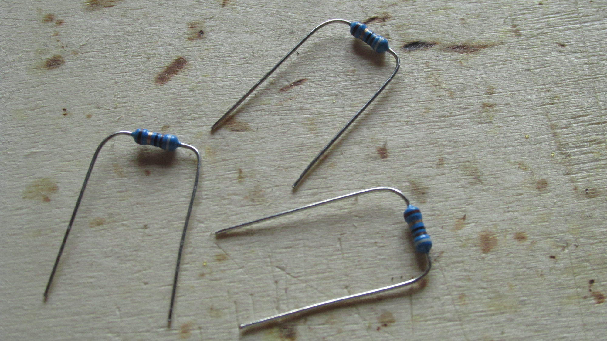
R3, R10, R23: Prepare form factor
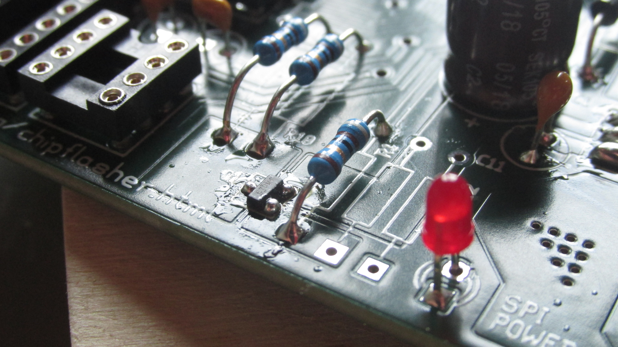
R3, R10, R23: Place on PCB, solder pins, cut leads, fix solder on component side if missing
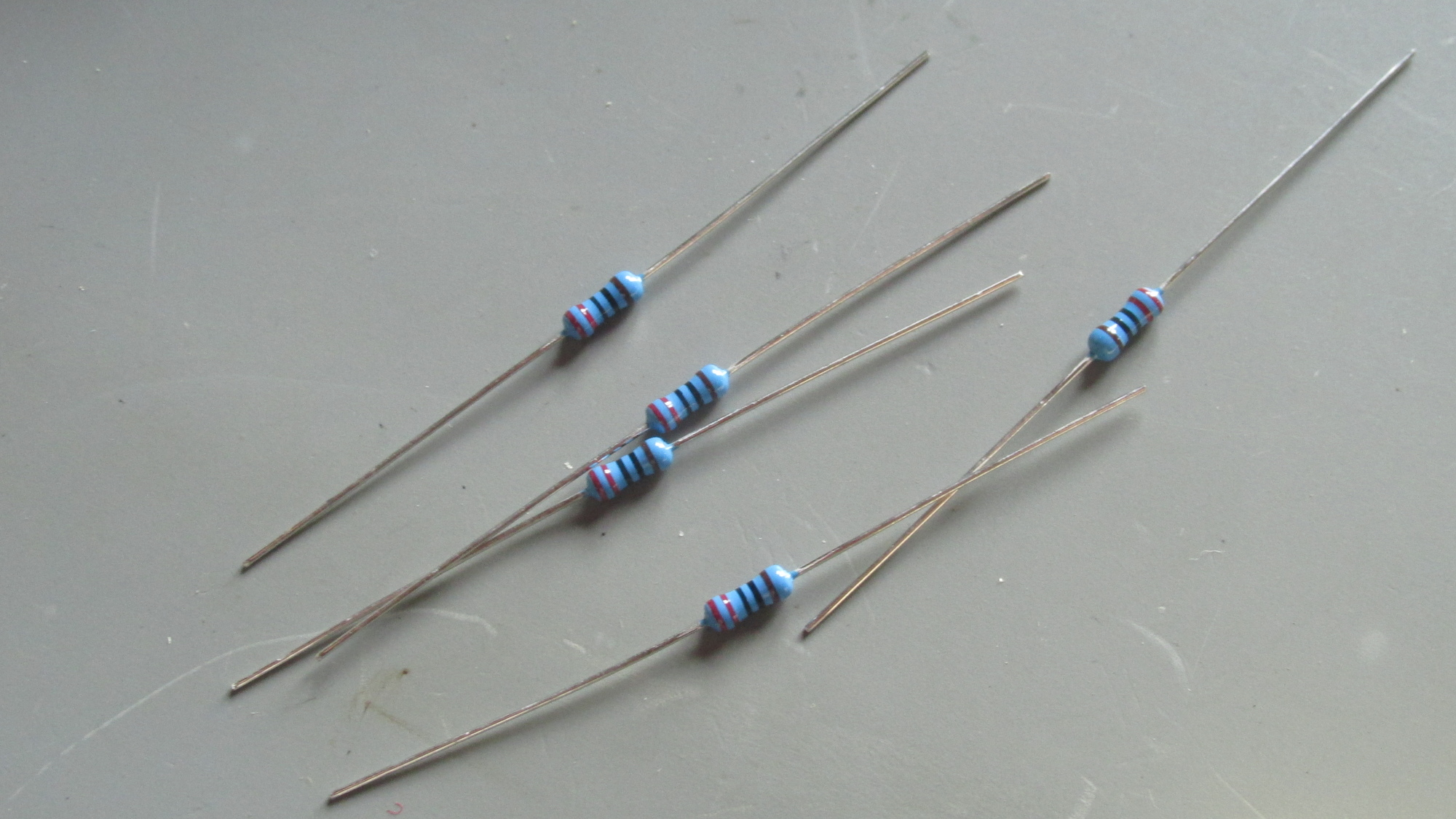
R15, R16, R17, R18, R22: Collect components, check color code
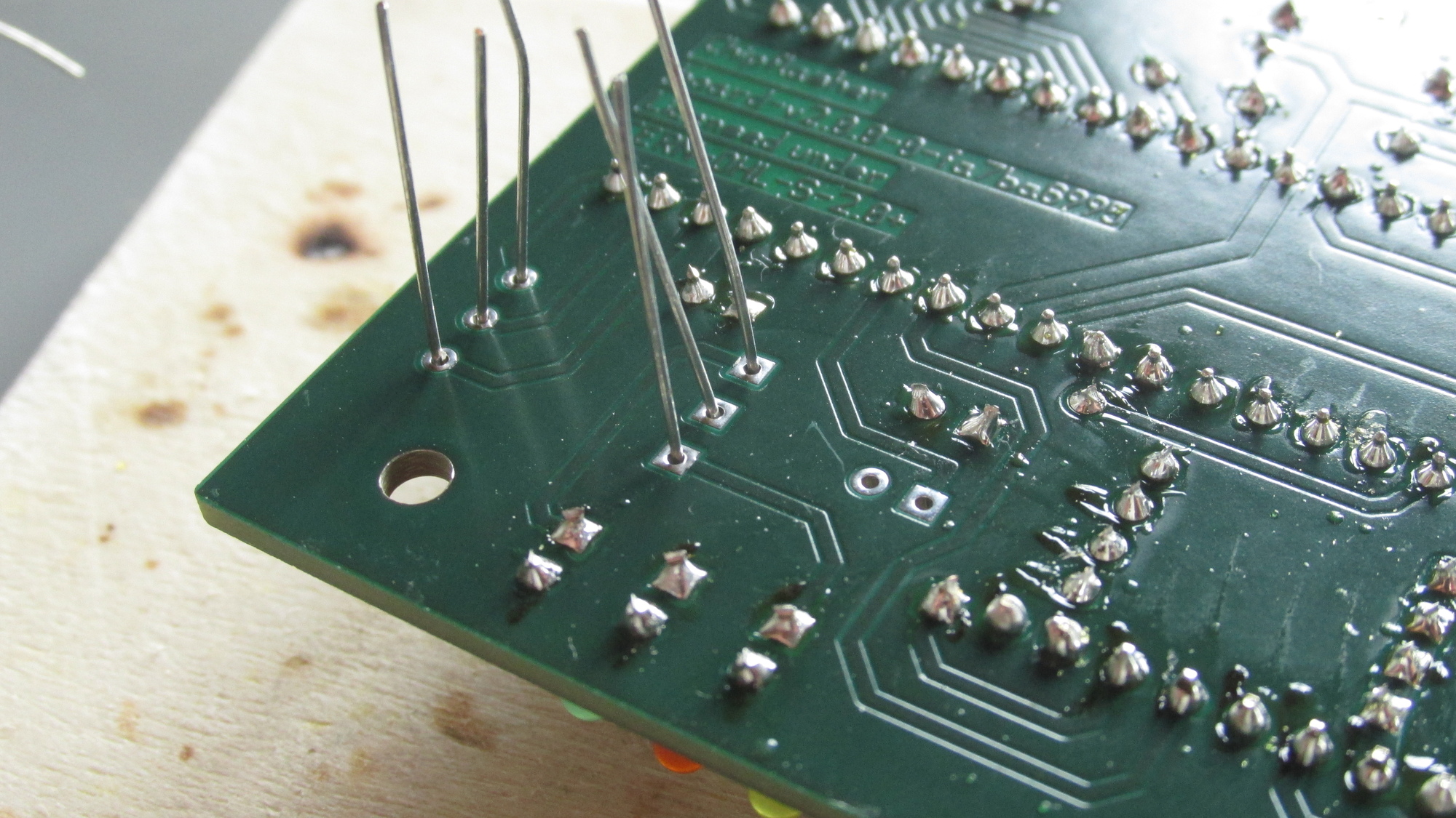
R15, R16, R17: Place components on PCB, spread leads slighly to make them remain in place
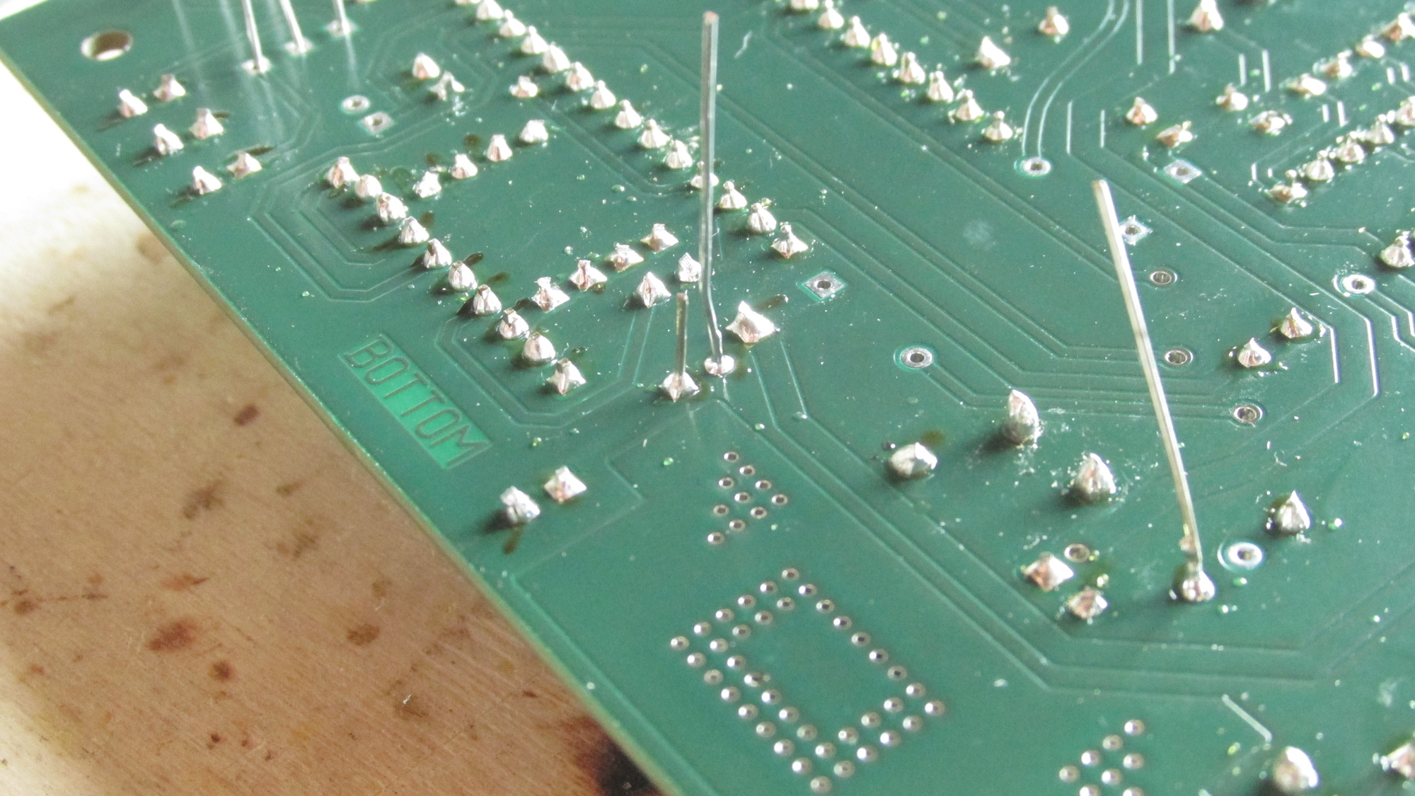
R18, R22: Apply solder on bottom side
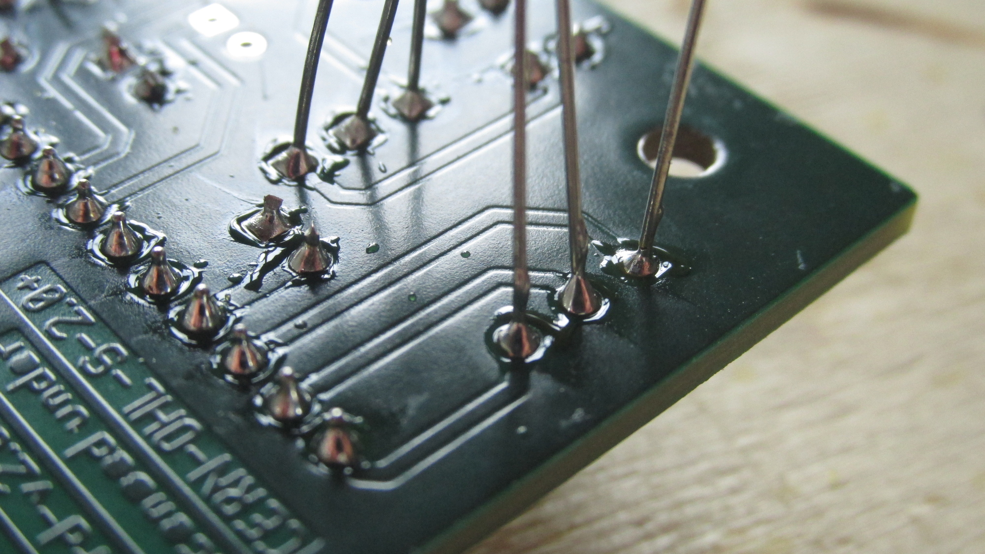
R15, R16, R17: Apply solder on bottom side
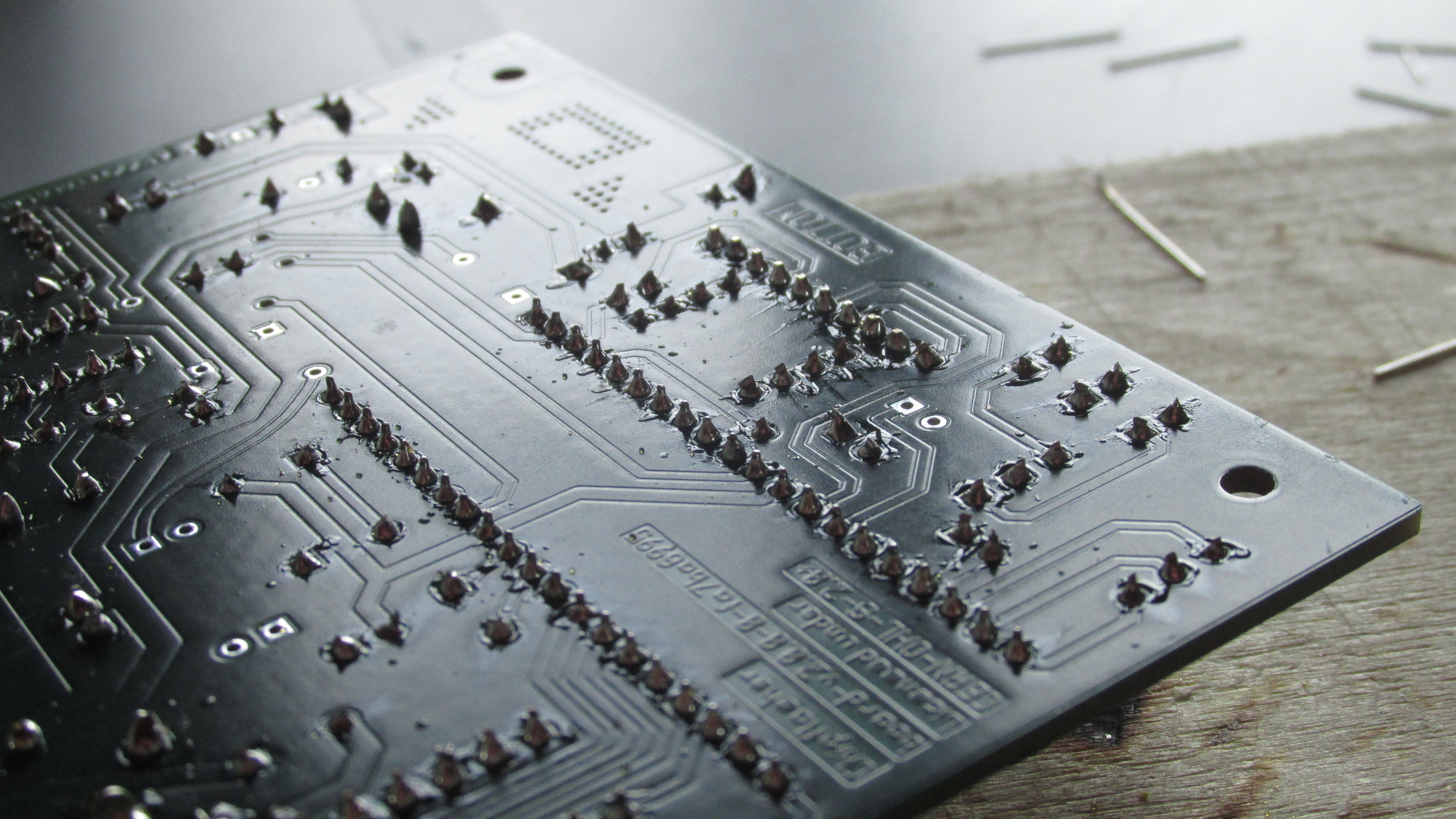
R15, R16, R17, R18, R22: Cut leads to make soldered pads look nice
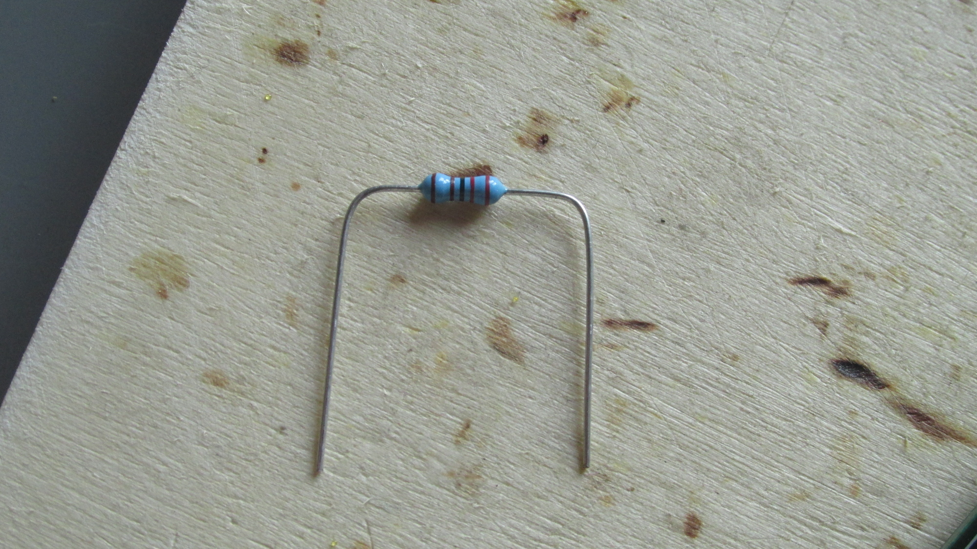
R21: Prepare form factor, check color code
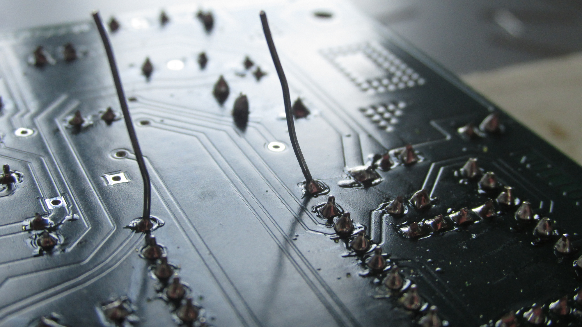
R21: Place component on PCB, solder pads
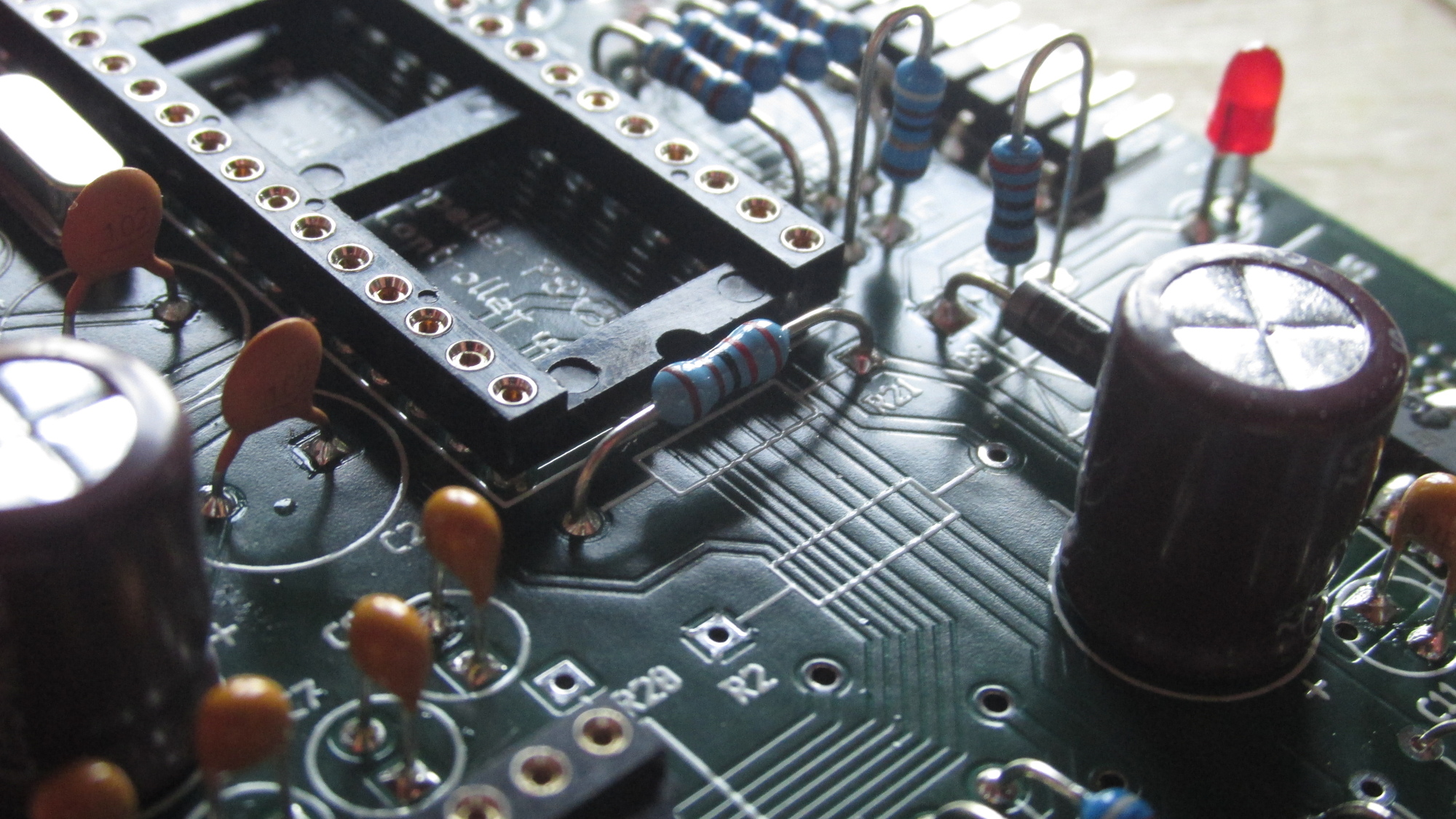
R21: Fix solder on component side, if necessary
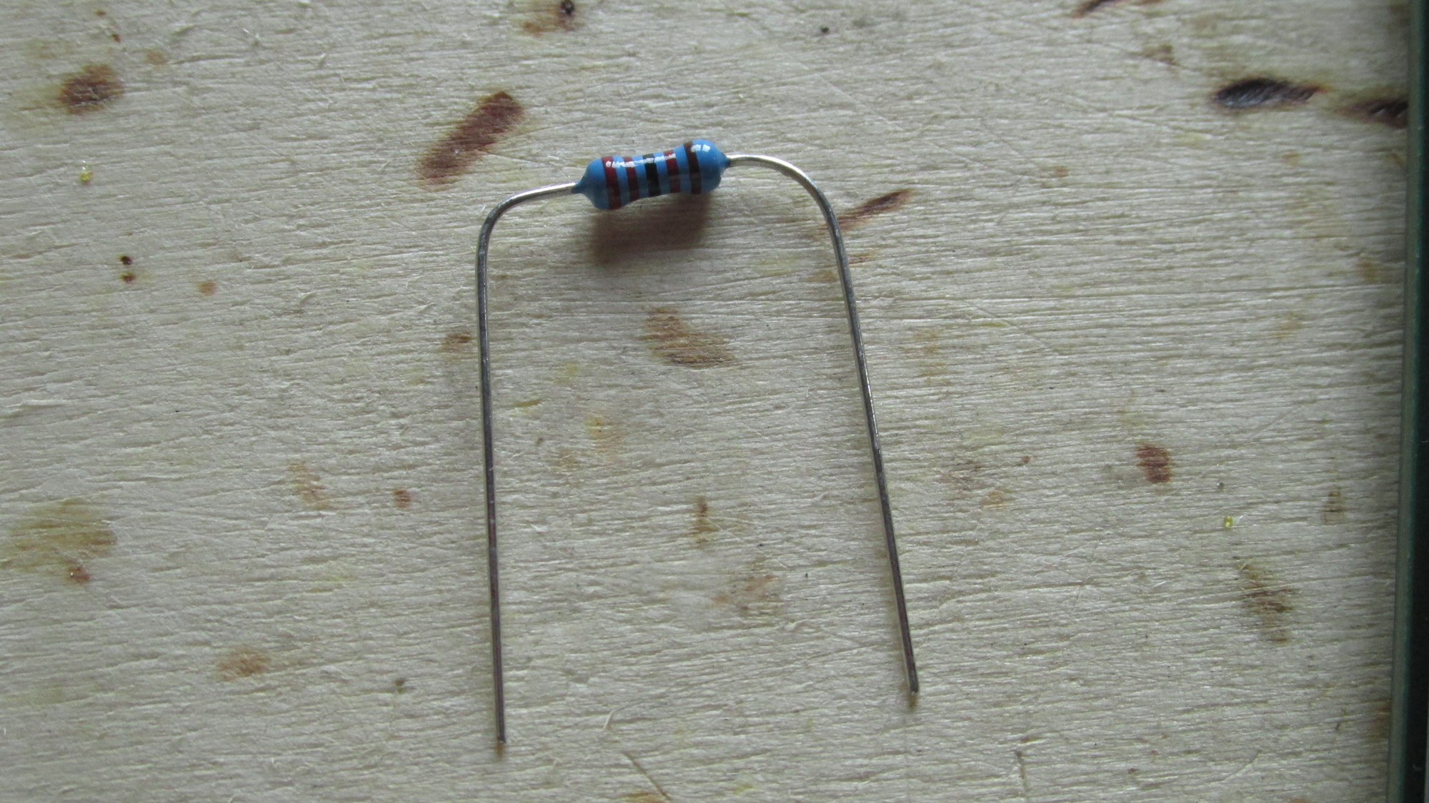
R2: Prepare form factor, check color code
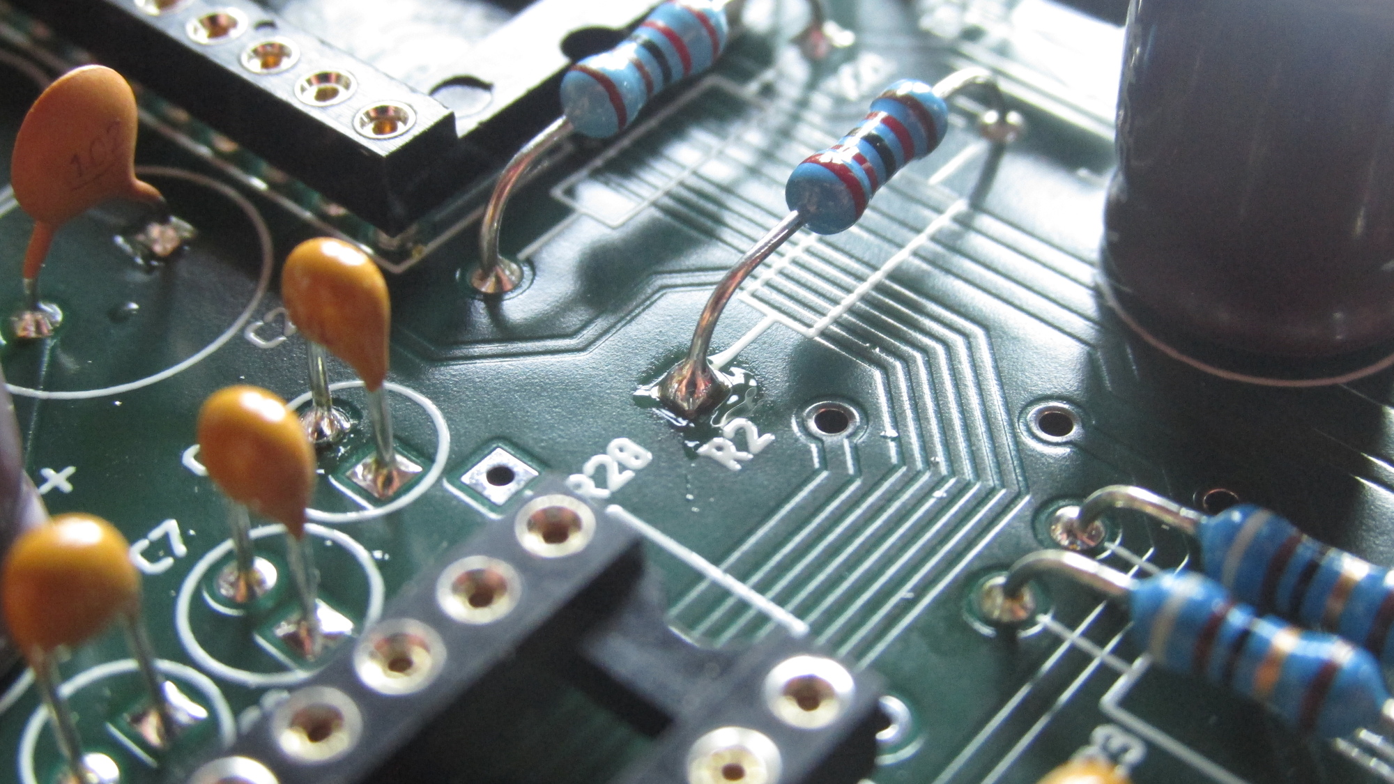
R2: Place on PCB, solder pads, cut leads, fix solder on component side
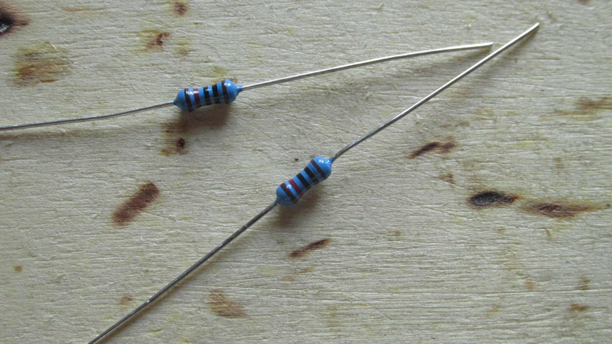
R19, R20: Collect components, check color code
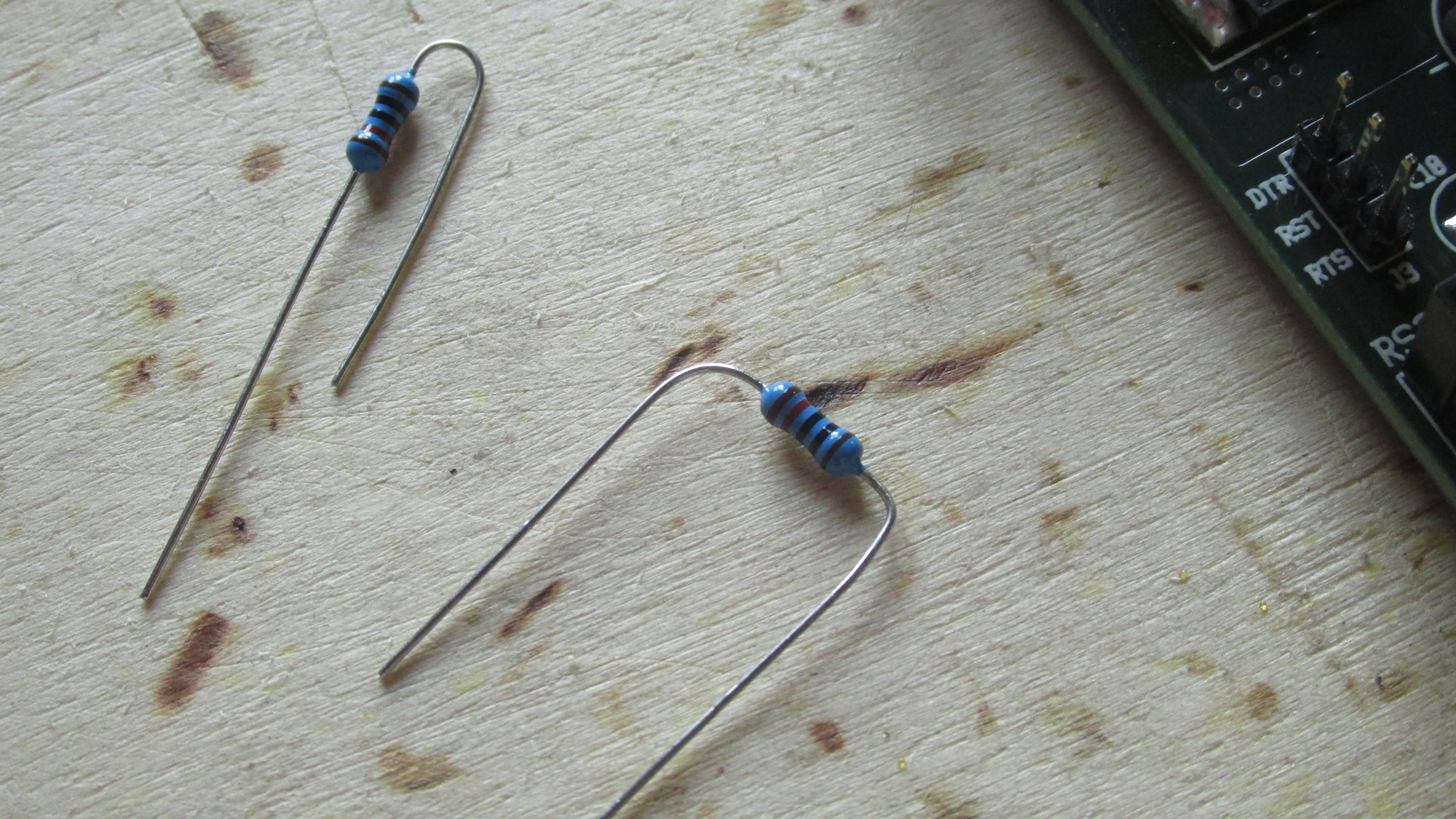
R19, R20: Prepare form factor
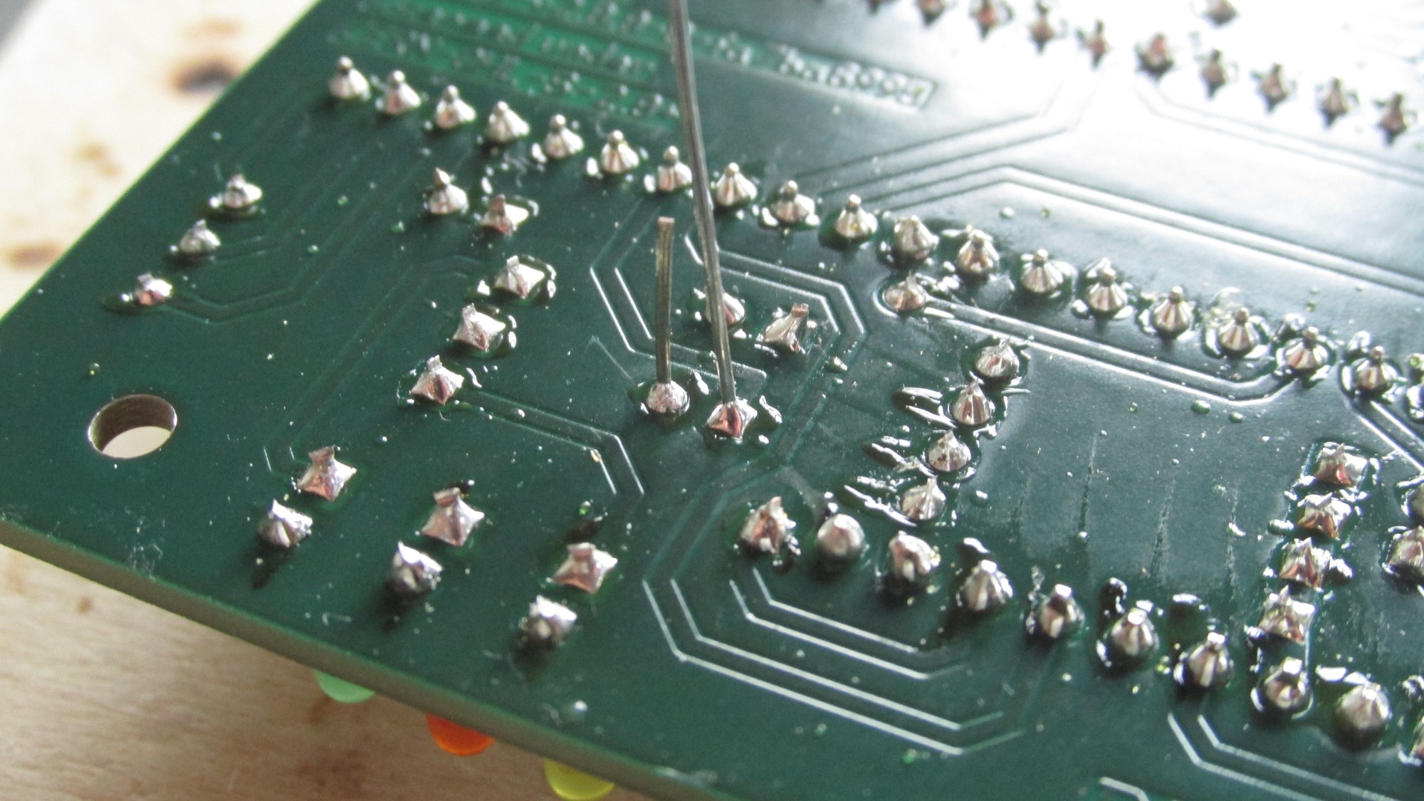
R19: Apply solder on bottom side, then cut leads
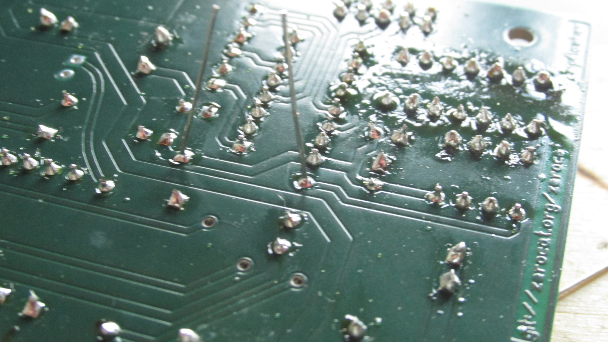
R20: Apply solder on bottom side, then cut leads
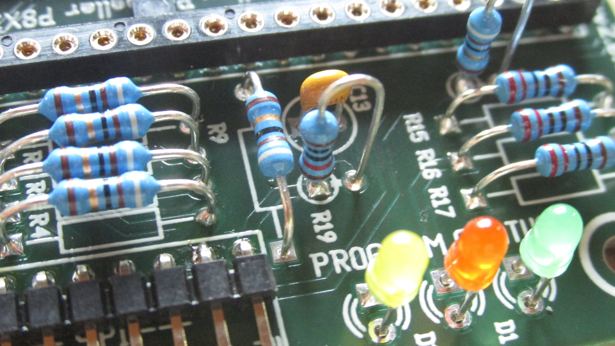
R19: Apply solder on component side, if necessary
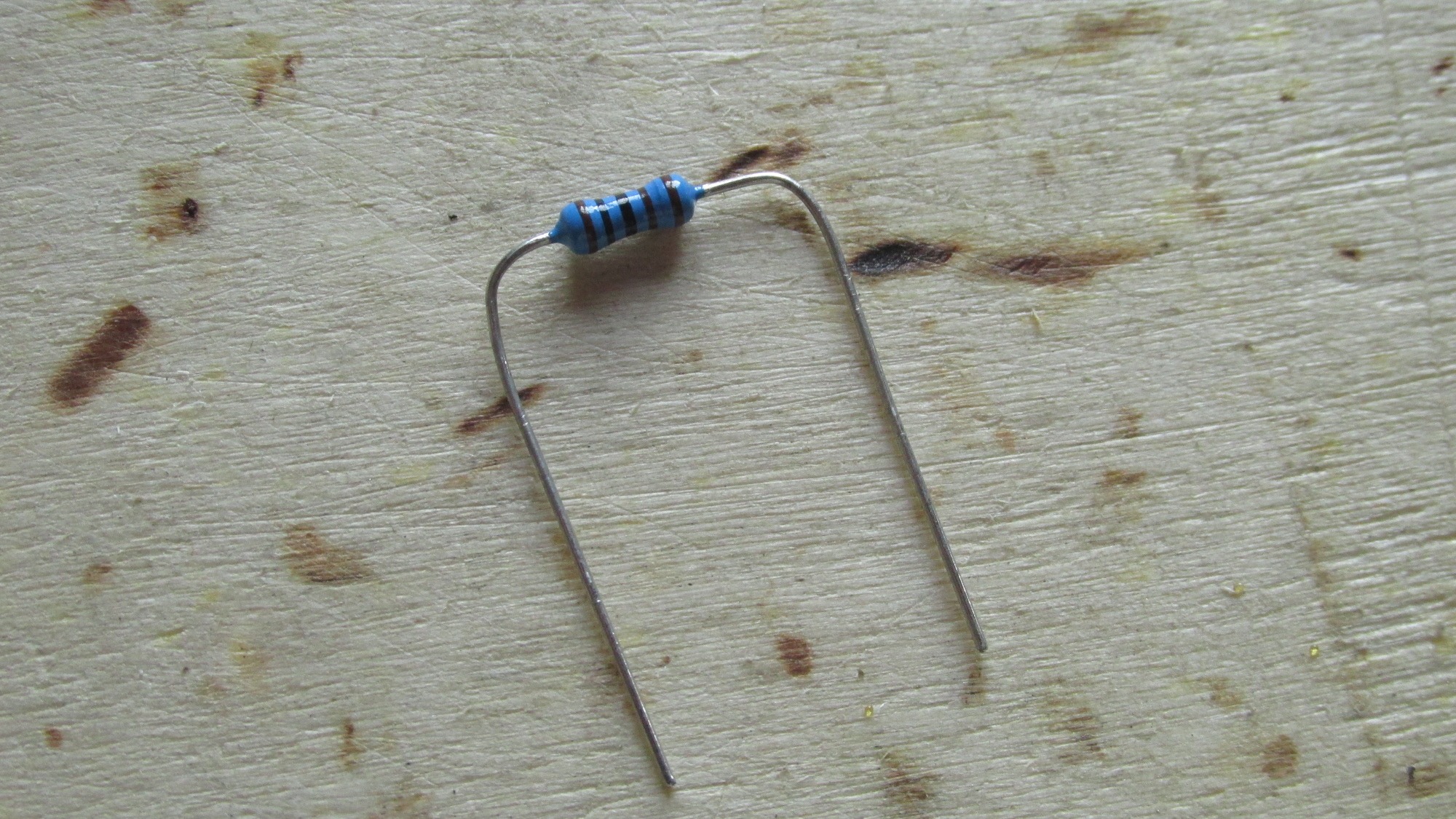
R1: Collect component, check color code
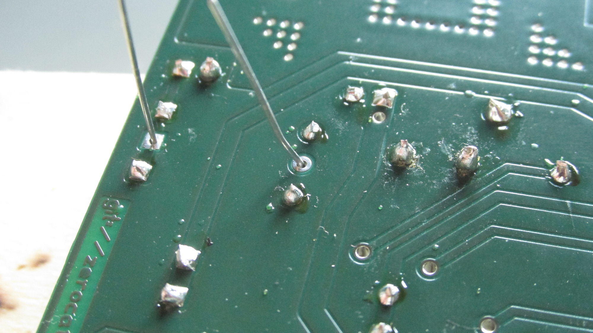
R1: Place on PCB, apply solder, cut leads, fix solder on component side
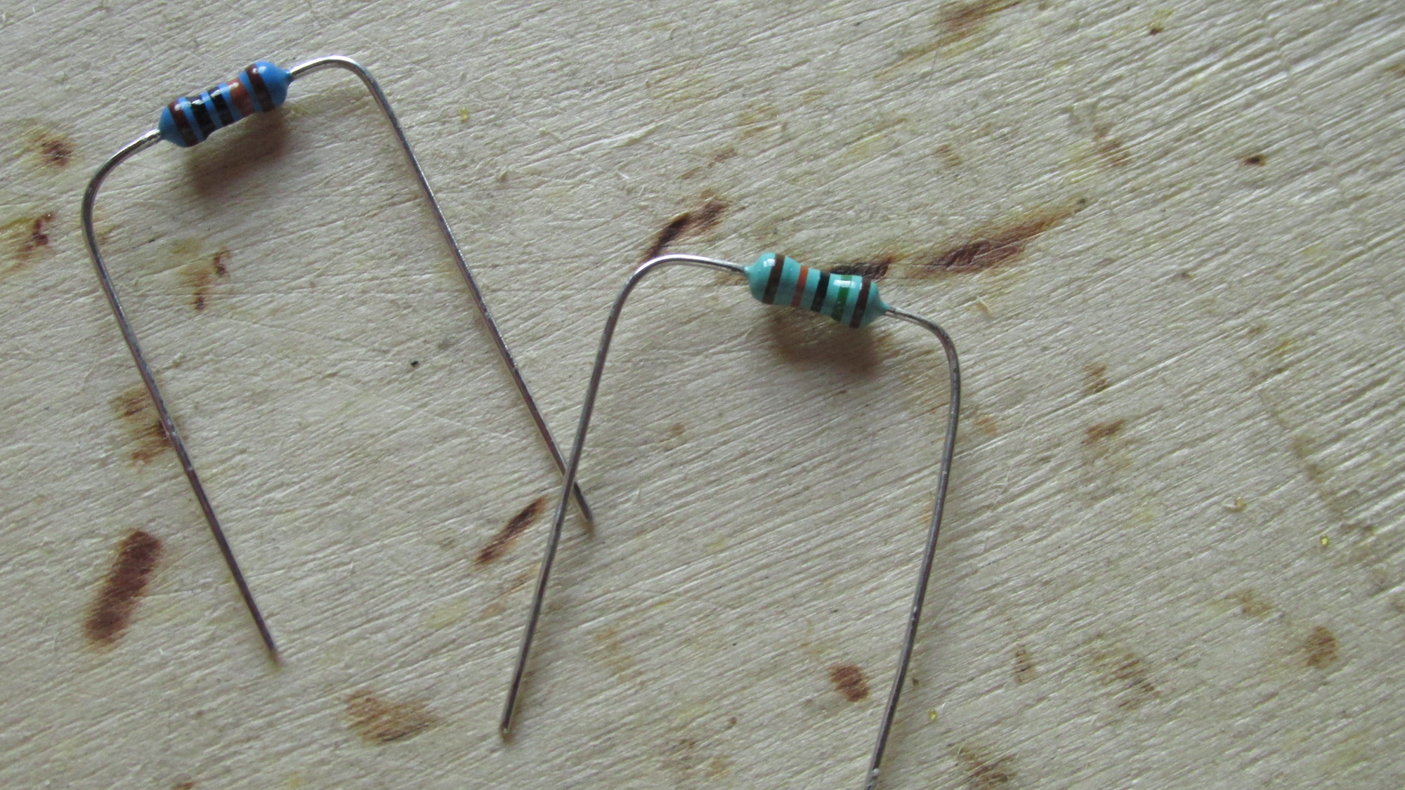
R13, R14: Collect components, check color codes, adjust form factor
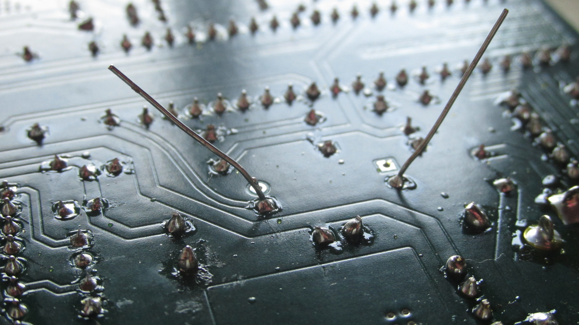
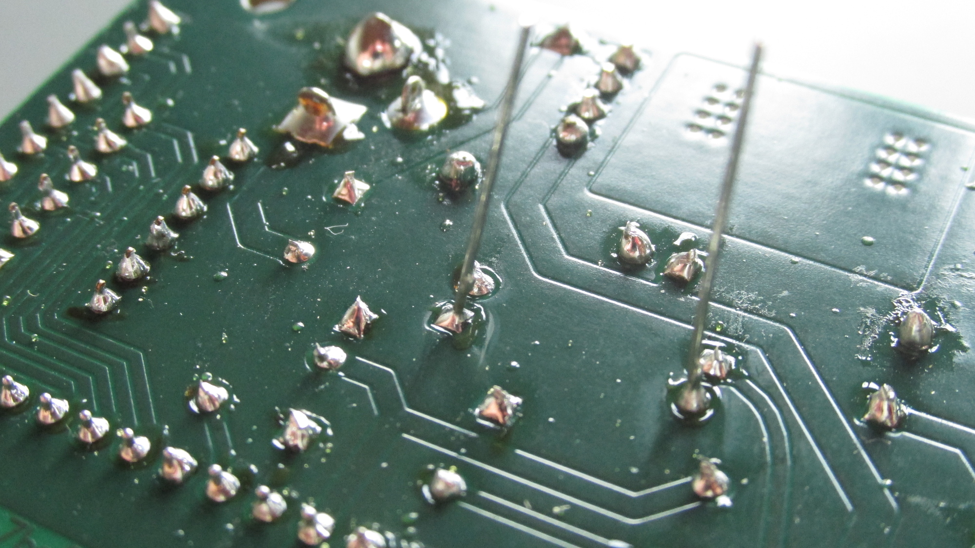
R14: Place component, apply solder on bottom side
R13: Place component, apply solder on bottom side
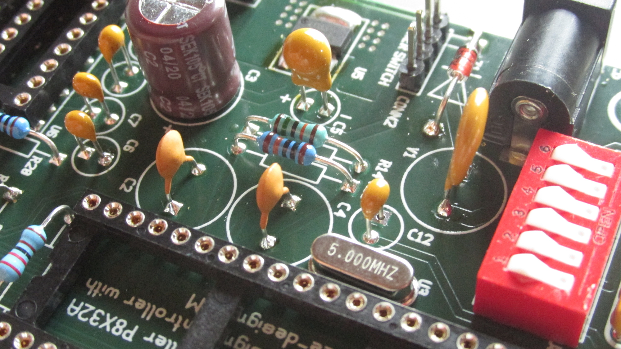
R13, R14: Fix solder on component side, if necessary
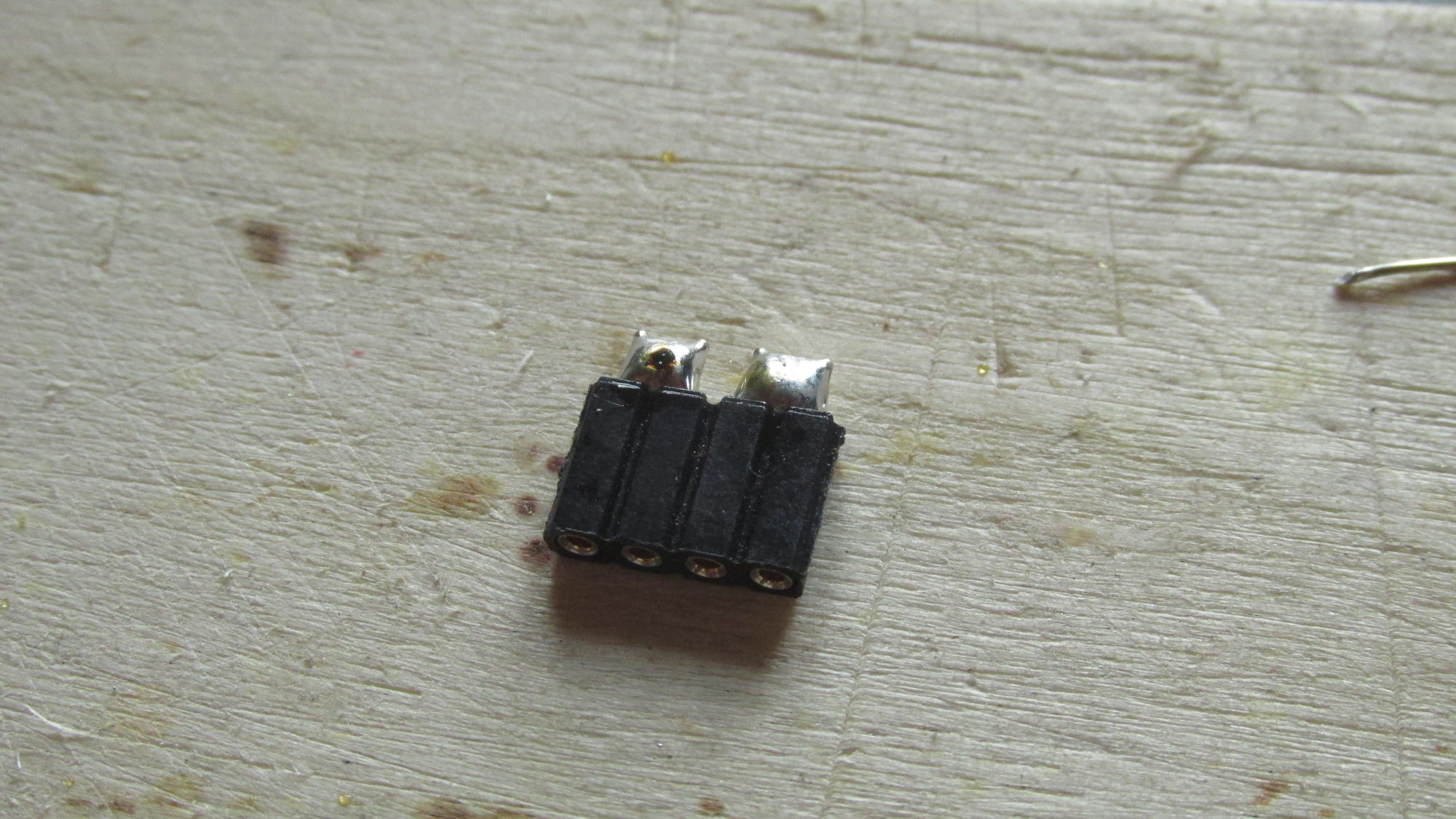
CONN2 Plug: Add solder to group of pins, use 1mm solder to be faster
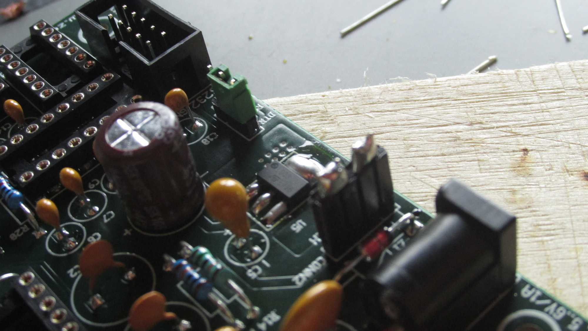
Plugs for CONN2 and J3: Place plugs onto pinheaders
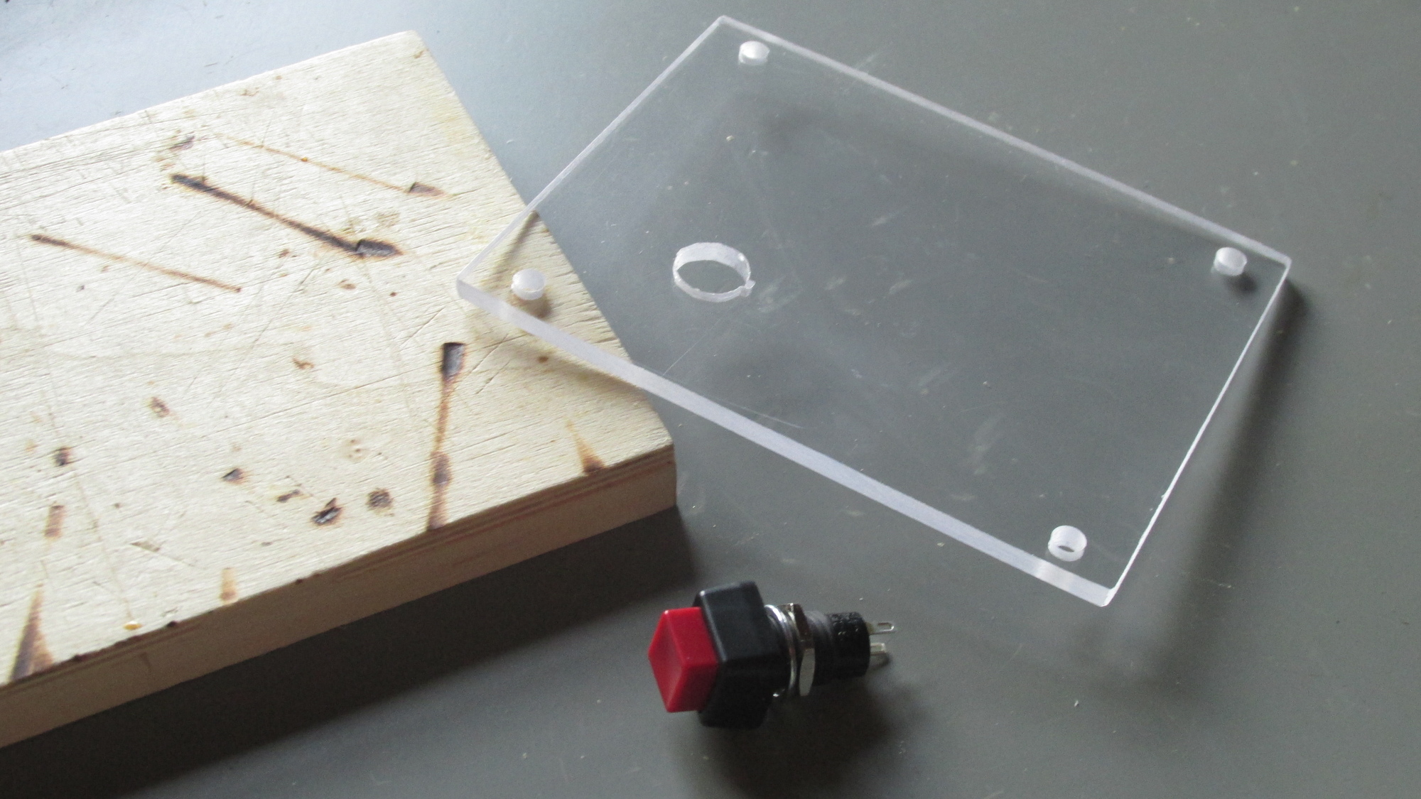
Panel: Collect Acrylic Glass and Power Switch
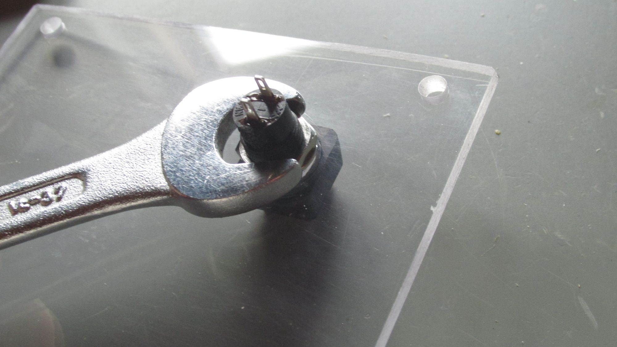
Panel: Mount Power Switch
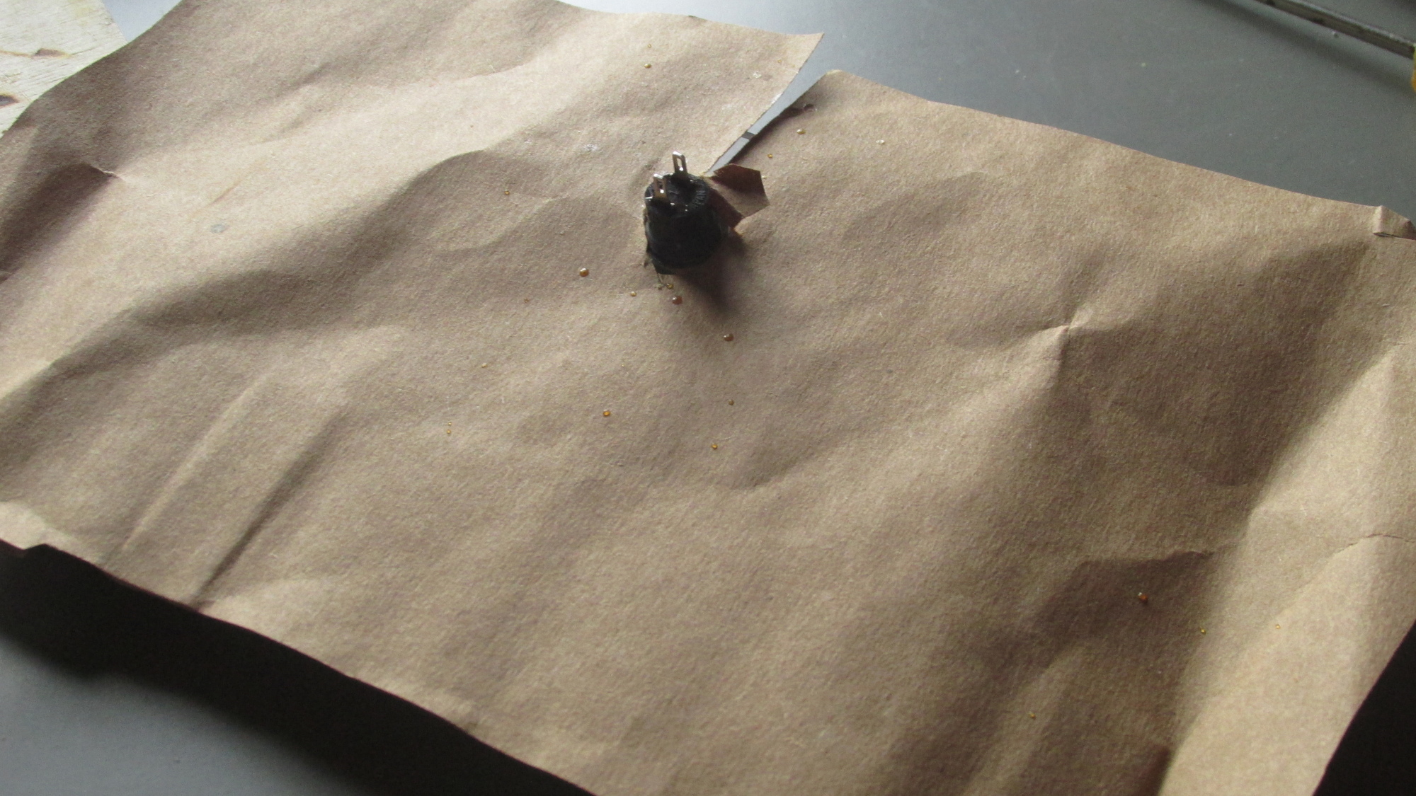
Panel: Protect Acrylic Glass with Cardboard
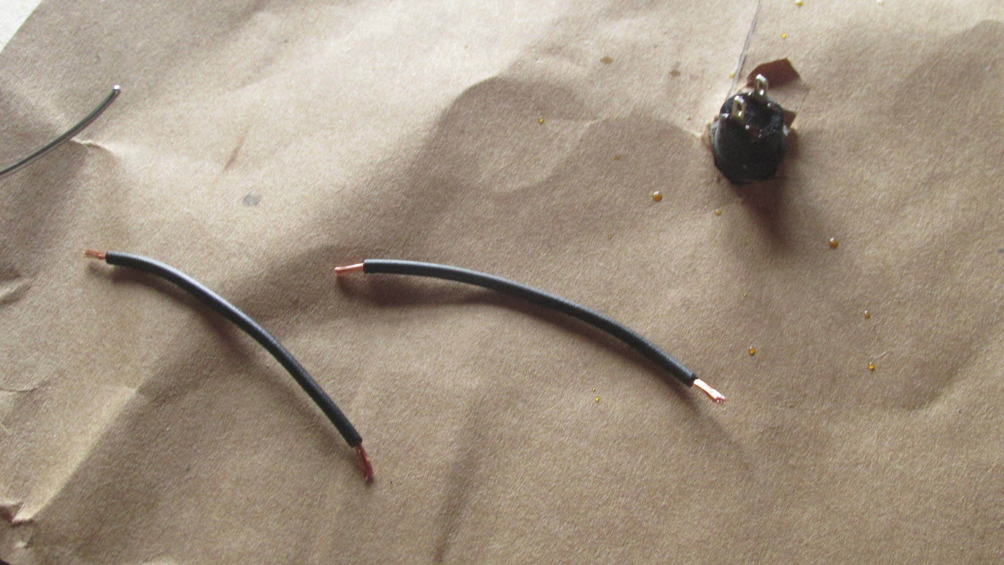
Panel: Prepare power wires and solder them to switch pins
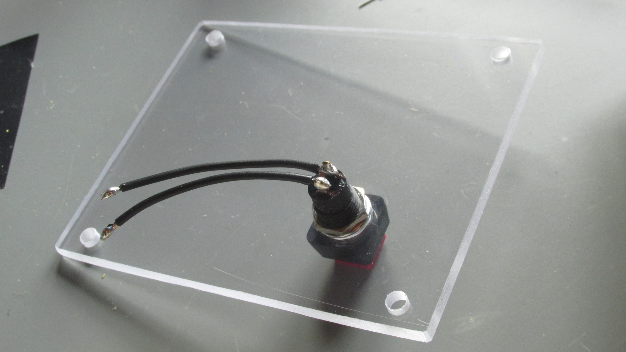
Panel: Remove cardboard
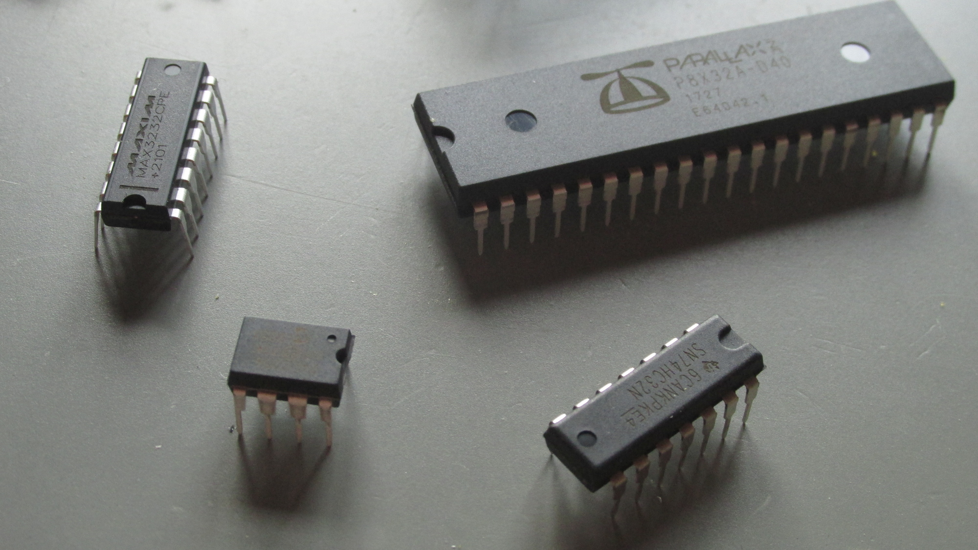
Microchips: Collect chips, observe precautions for electrostatic sensitive devices!
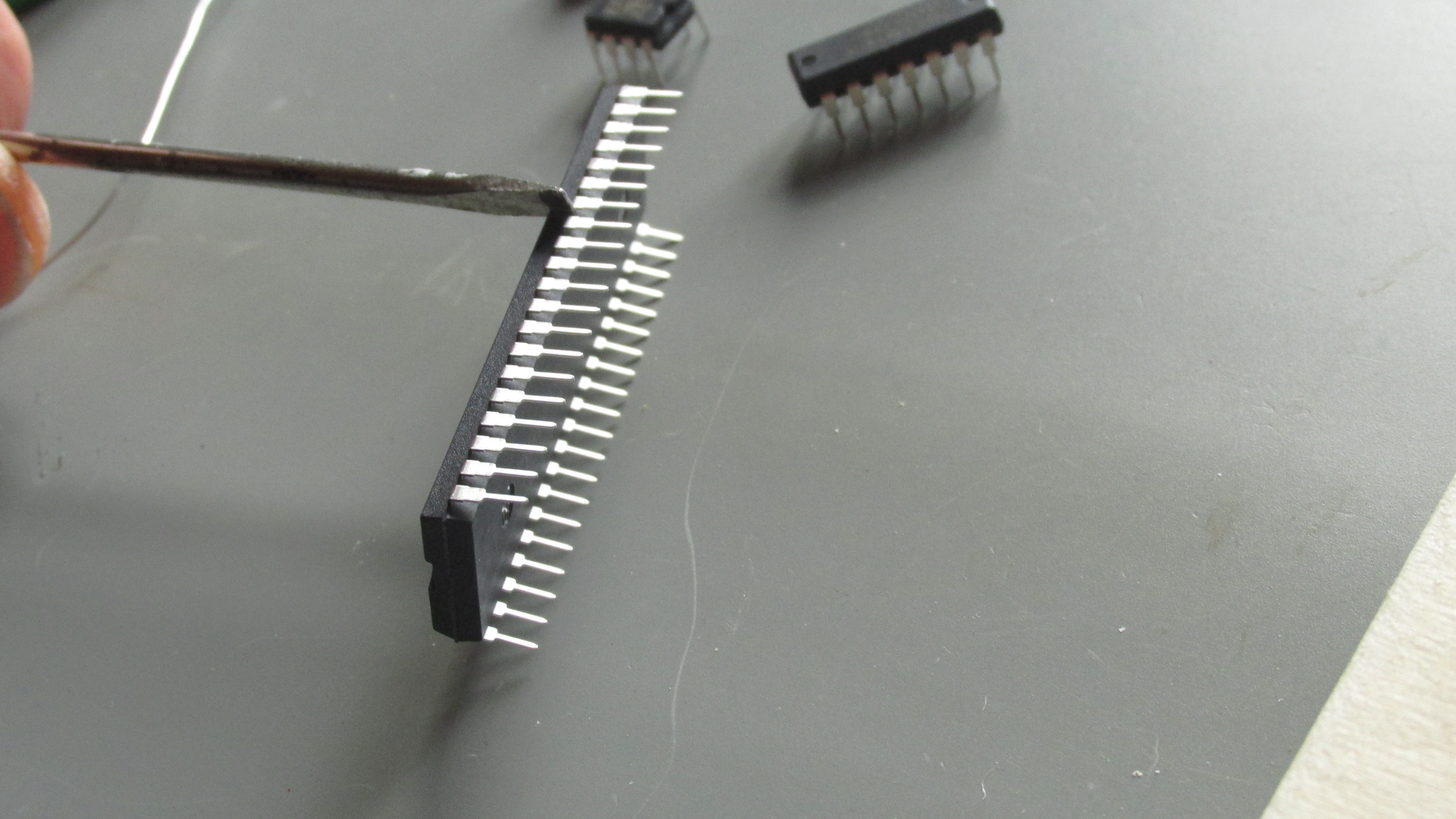
Microchips: Press chip down on flat surface in order to put pins towards 90° angle
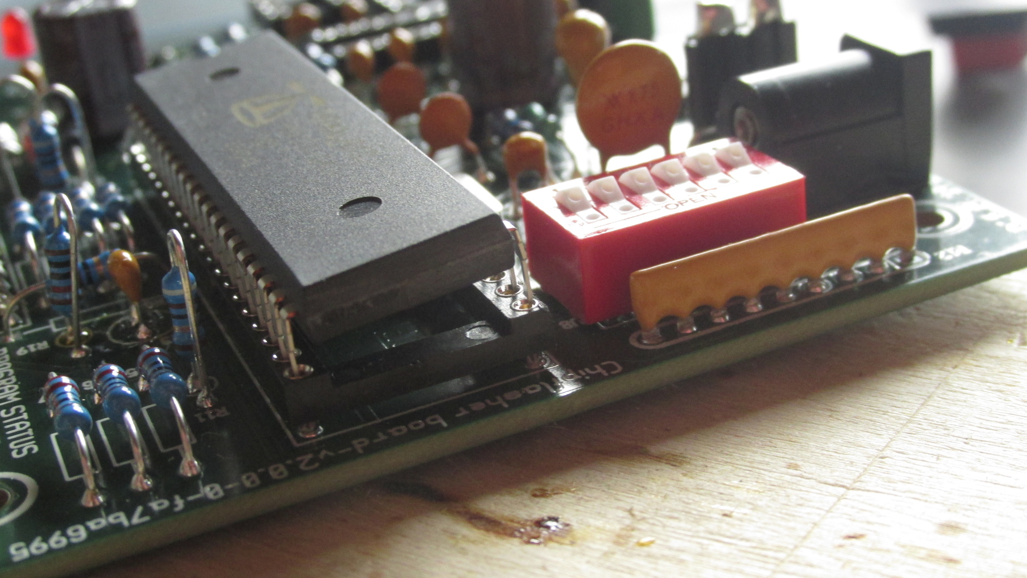
Microchips: Sort all pins into socket until chip is horizontal, then press down
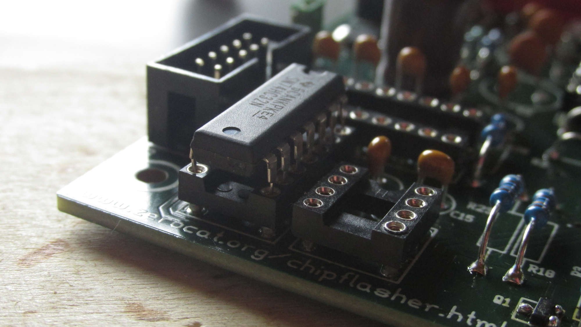
Microchips: Sort pins into socket ...
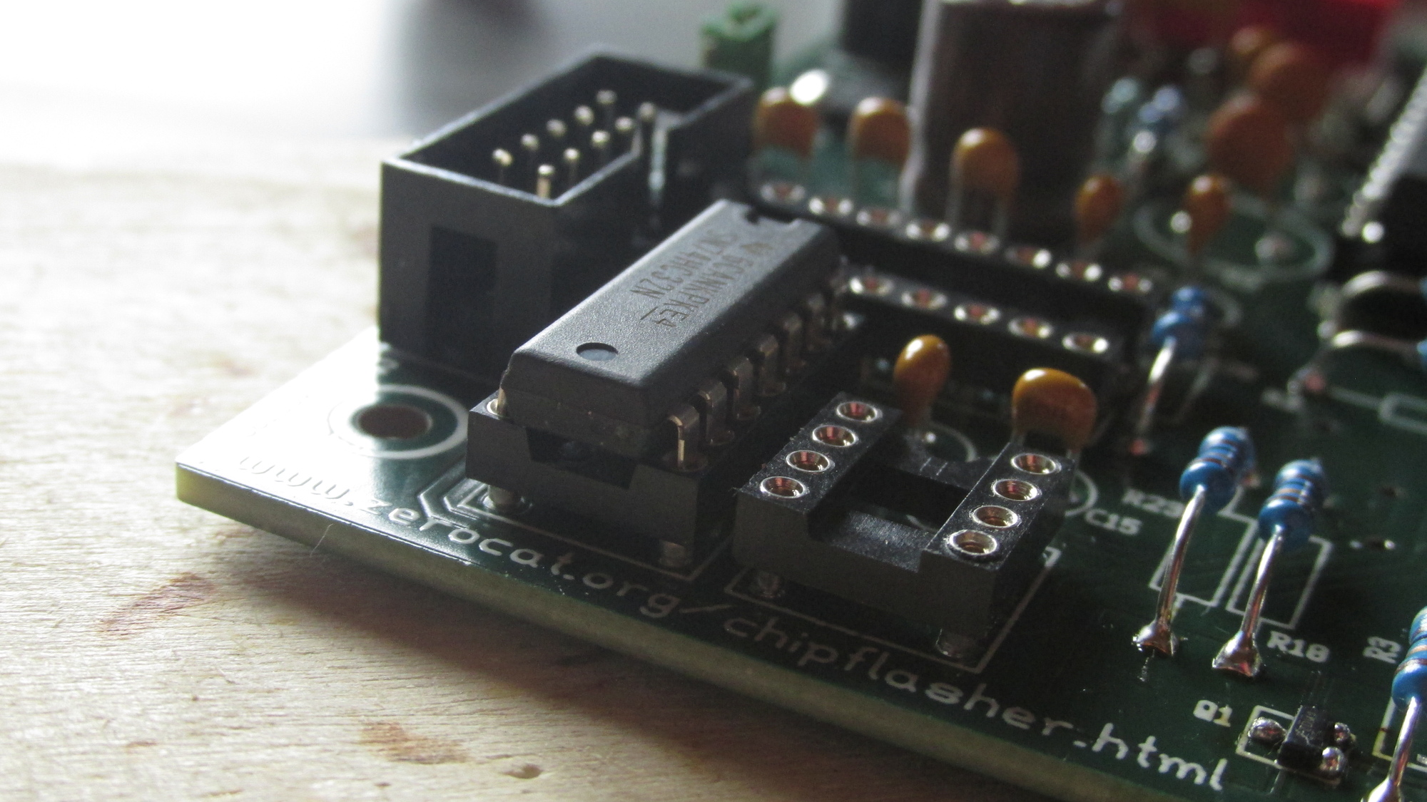
Microchips: .. then press down
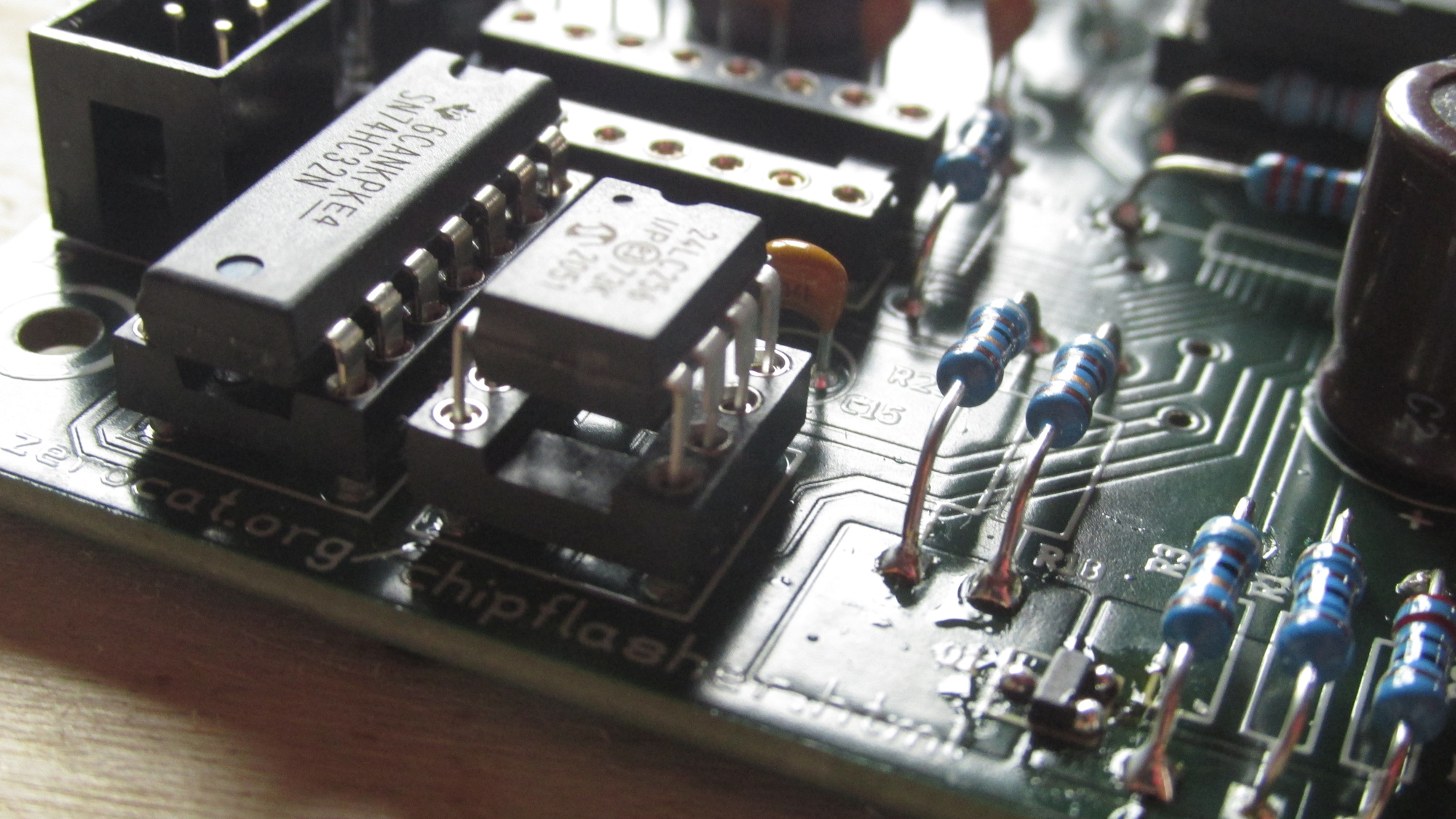
Microchips: Sort pins into socket ...
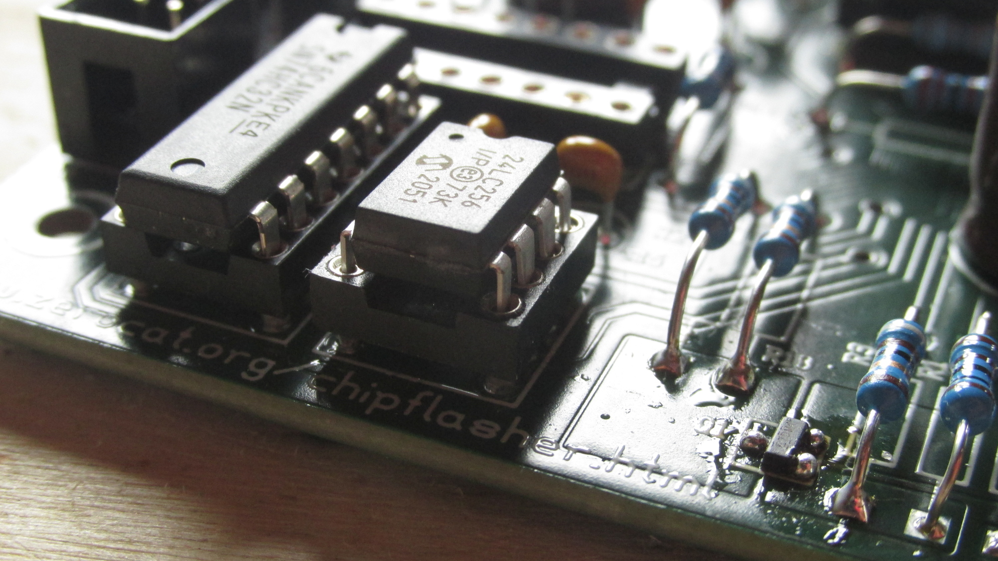
Microchips: ... then press down
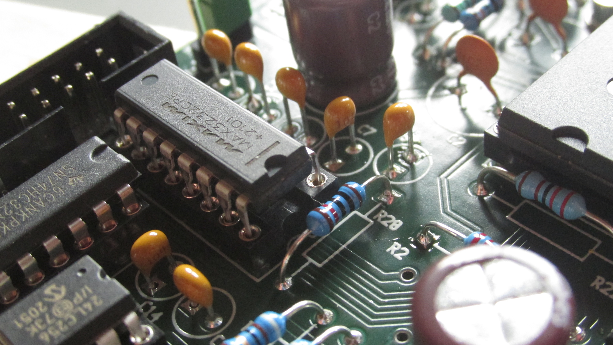
Microchips: Sort pins into socket ...
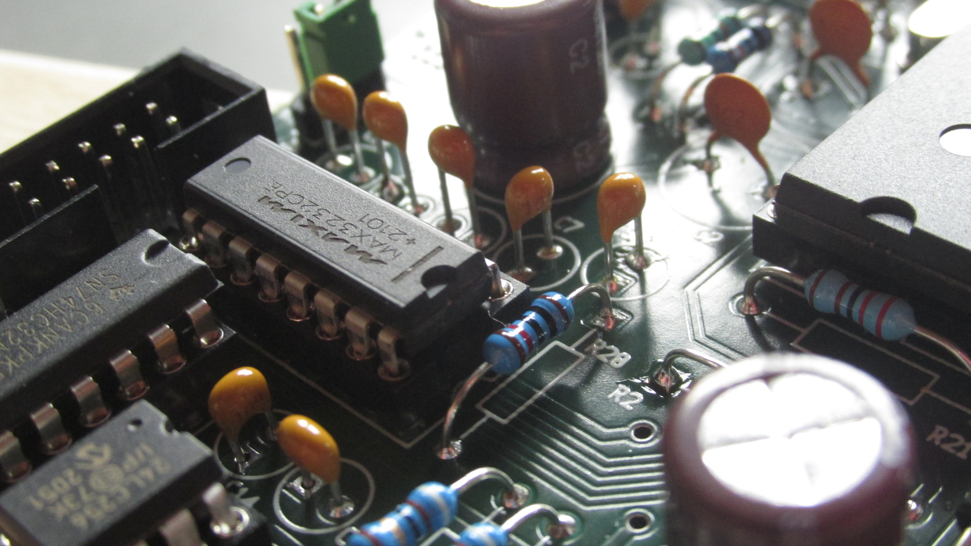
Microchips: ... then press down
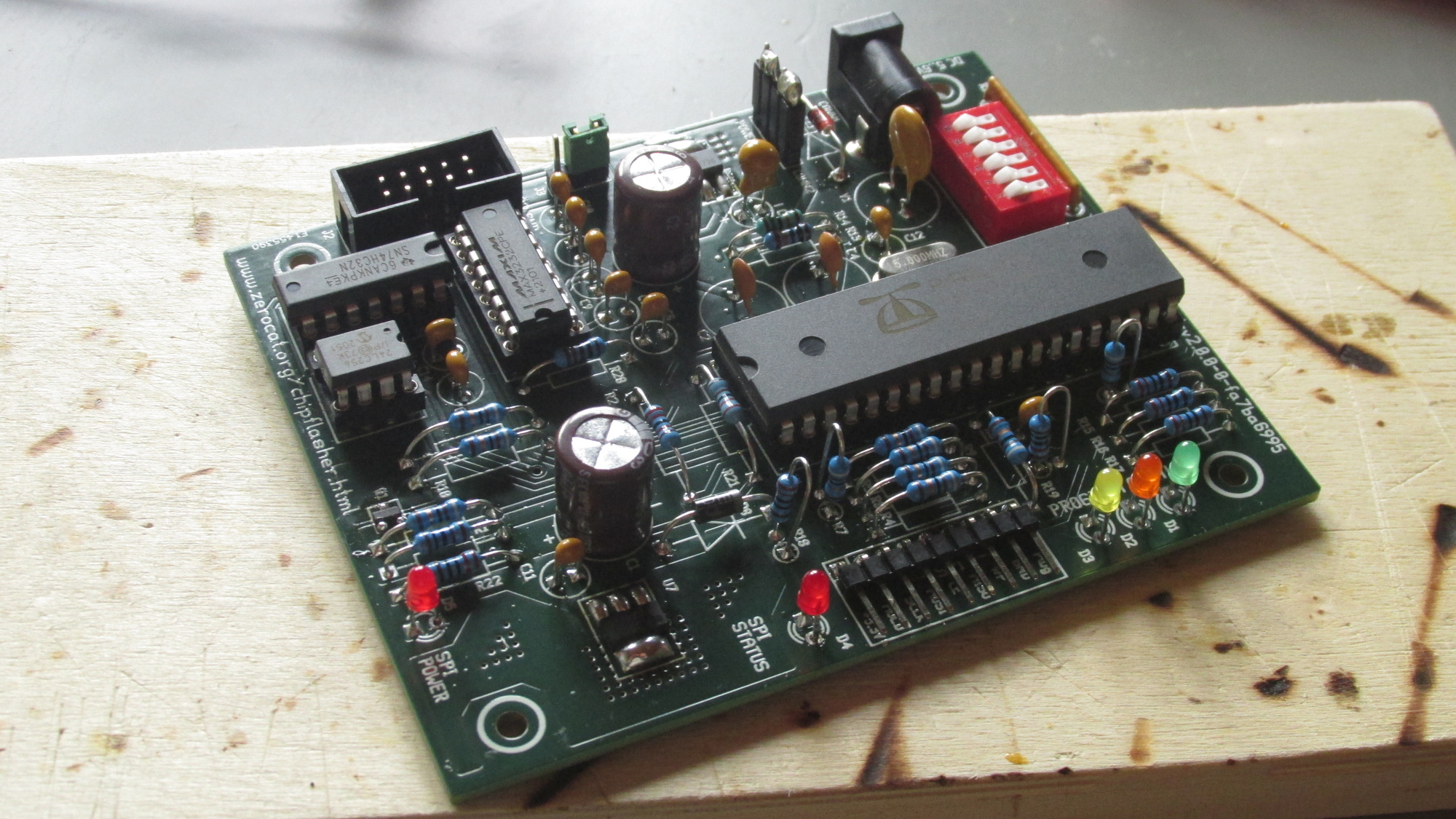
PCB fully populated, done!
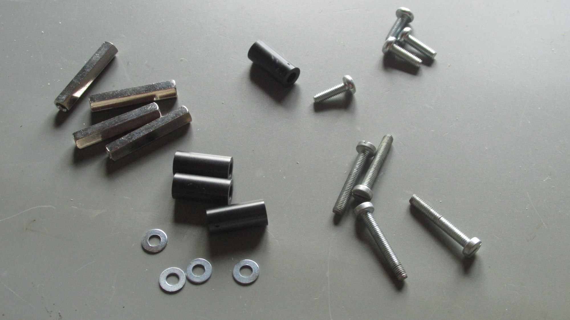
Chassis: Collect bolts and screws and mount them to the PCB
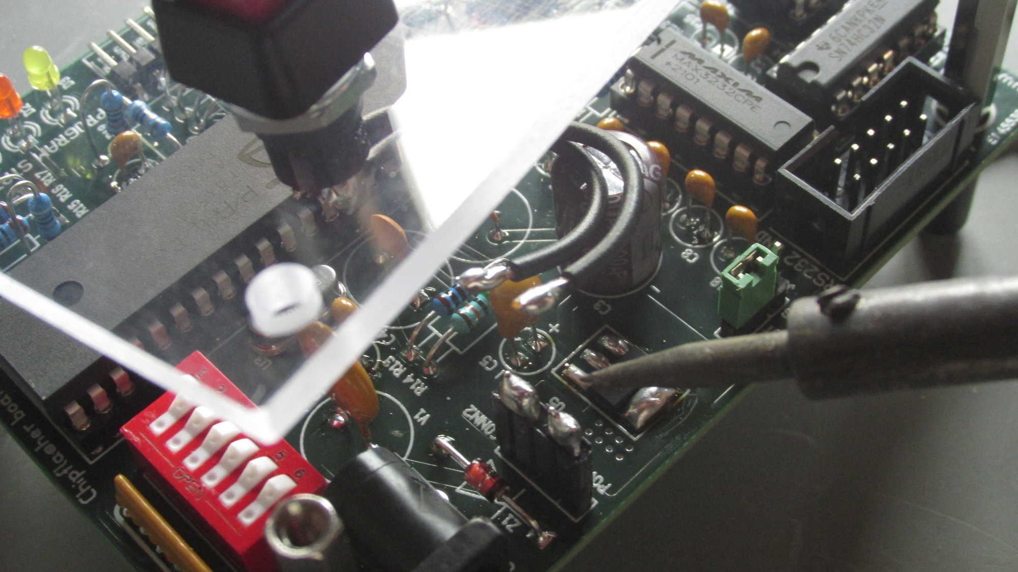
Chassis: Grab Device Panel and solder Power Switch Cables ...
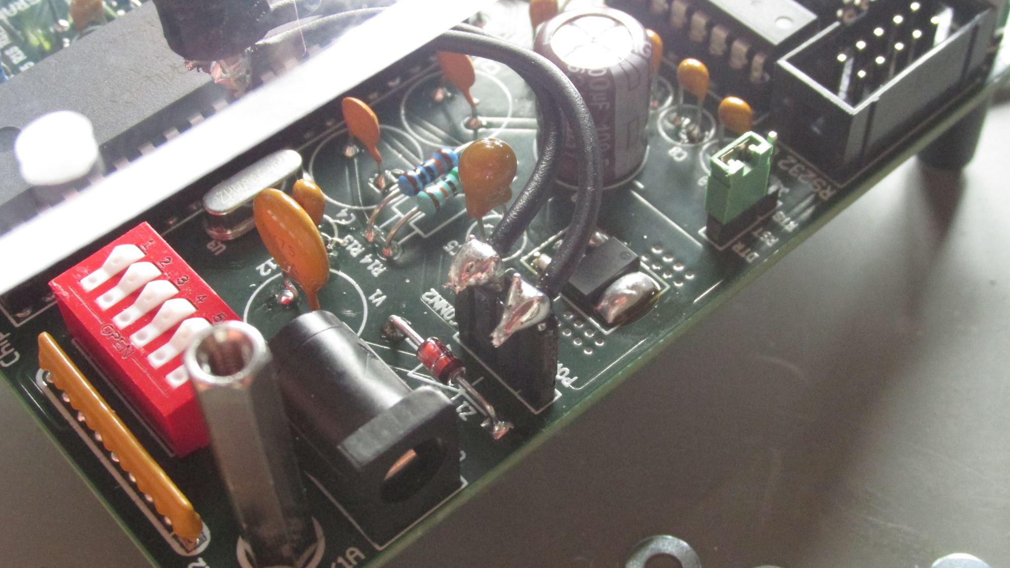
Chassis: ... to CONN1 Plug
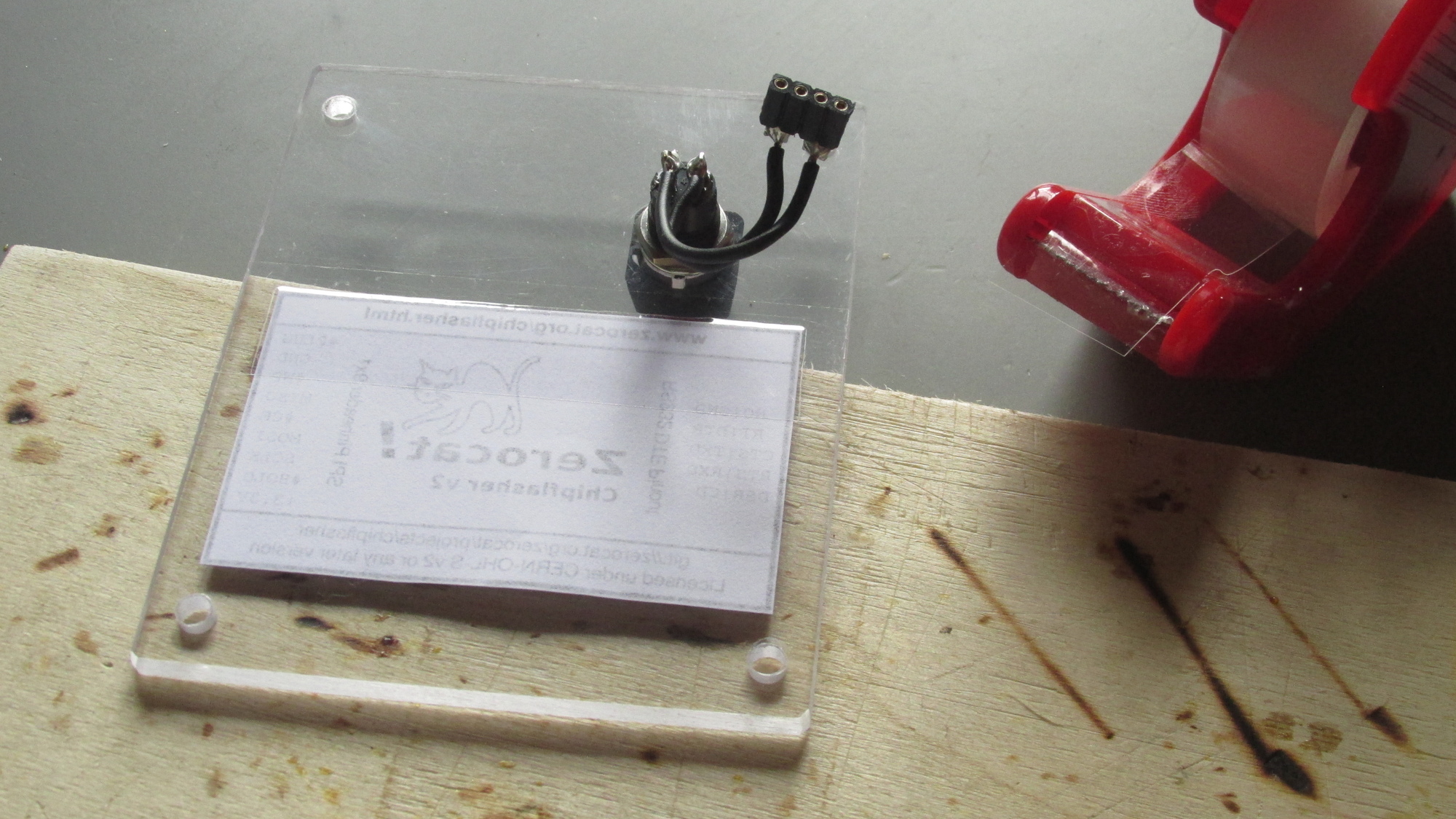
Chassis: Unplug Power Switch, fix label with transparent tape below glass
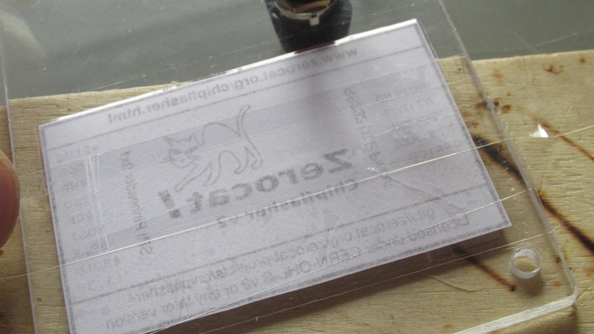
Chassis: Use multiple stripes to seal paper
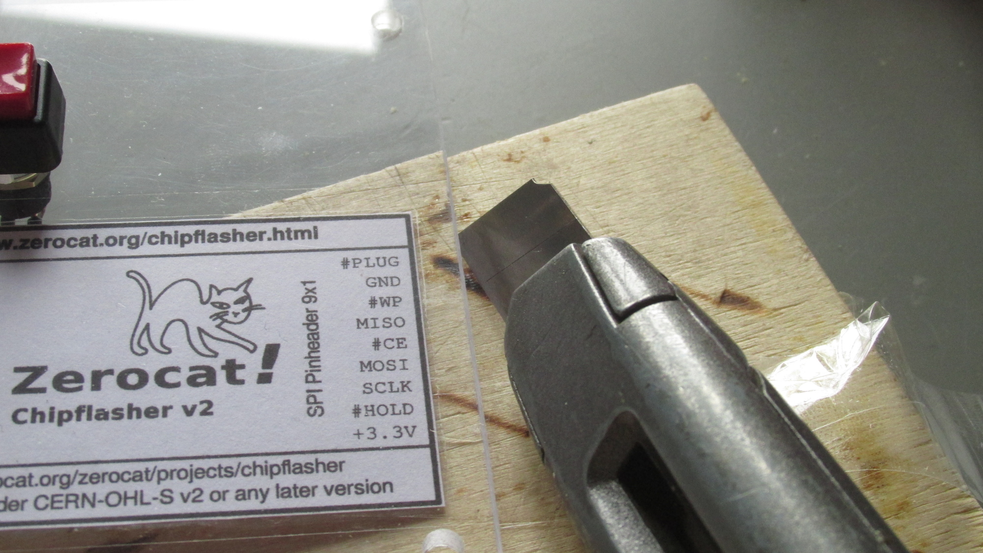
Chassis: Flip panel, cut stripes along edge
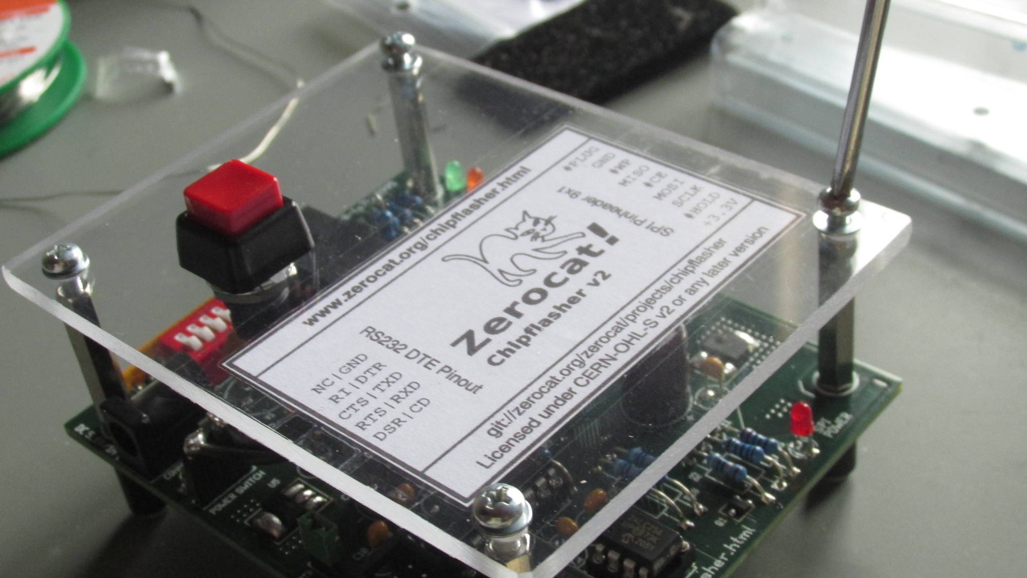
Chassis: Mount panel with screwdriver, apply Power Switch Plug
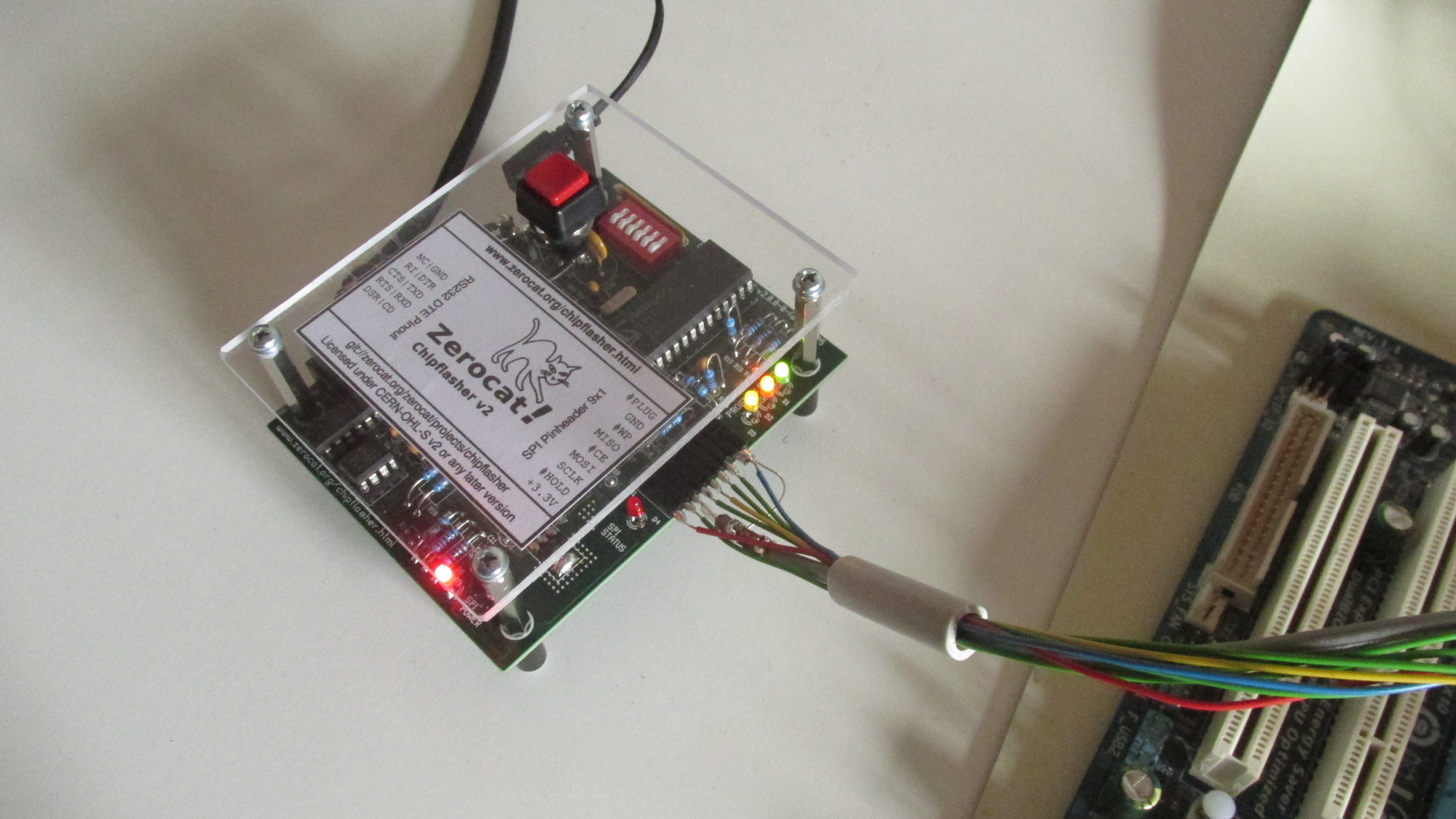
Device Test: Power on (D5 lights up), Firmware upload (D1..D3 blink two times)
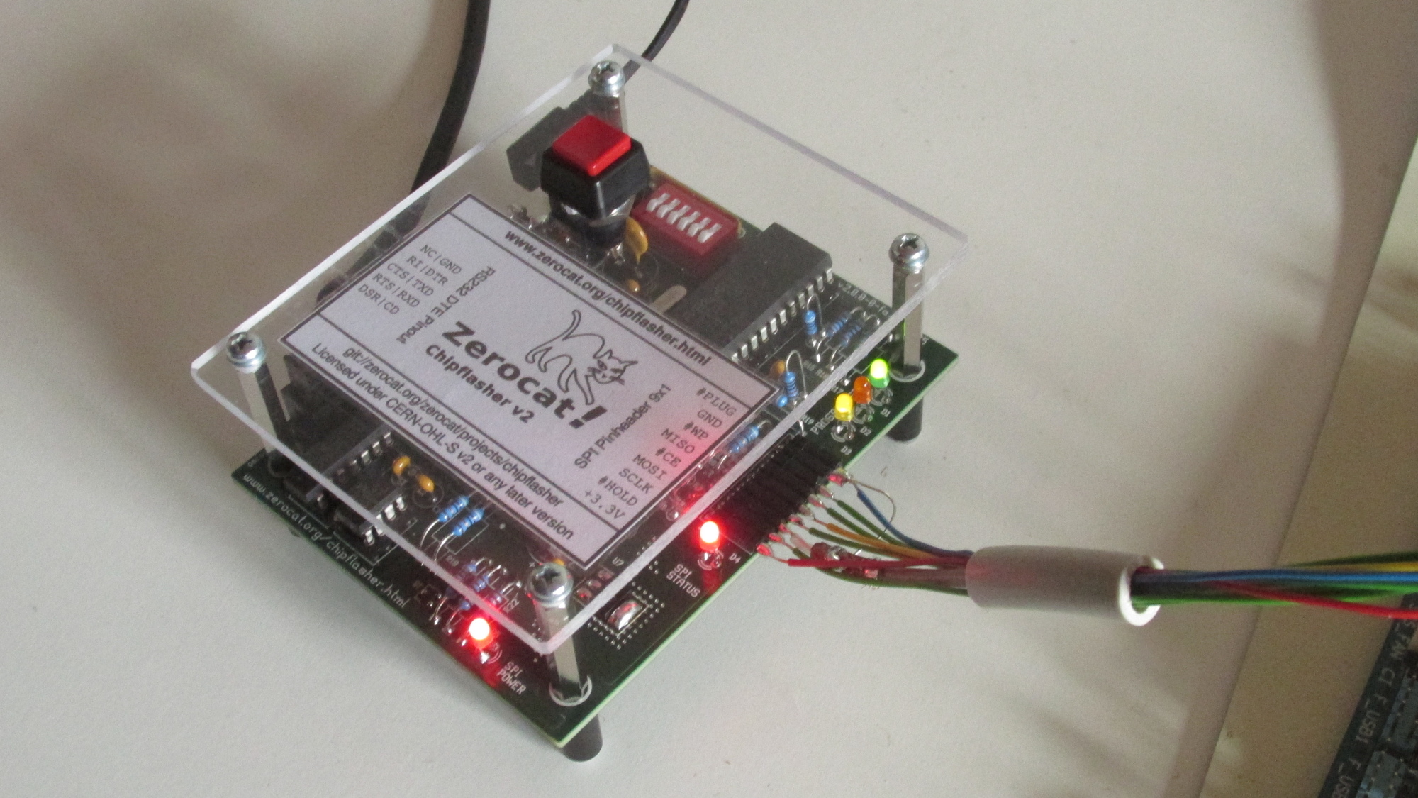
Device Test: Flashrom Probe (D4 lights up)
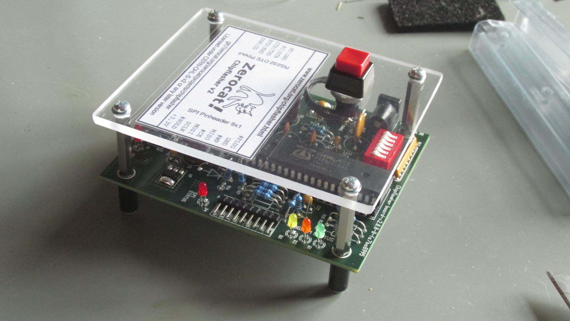
Chipflasher v2 is ready to use!
Eurocircuits is a professional PCB manufacturer, which has been chosen to process the exported chipflasher ZIP archive. In October 2022, an order of 10 PCBs was processed in no time, resulting in high quality PCBs and one extra PCB as a gift!
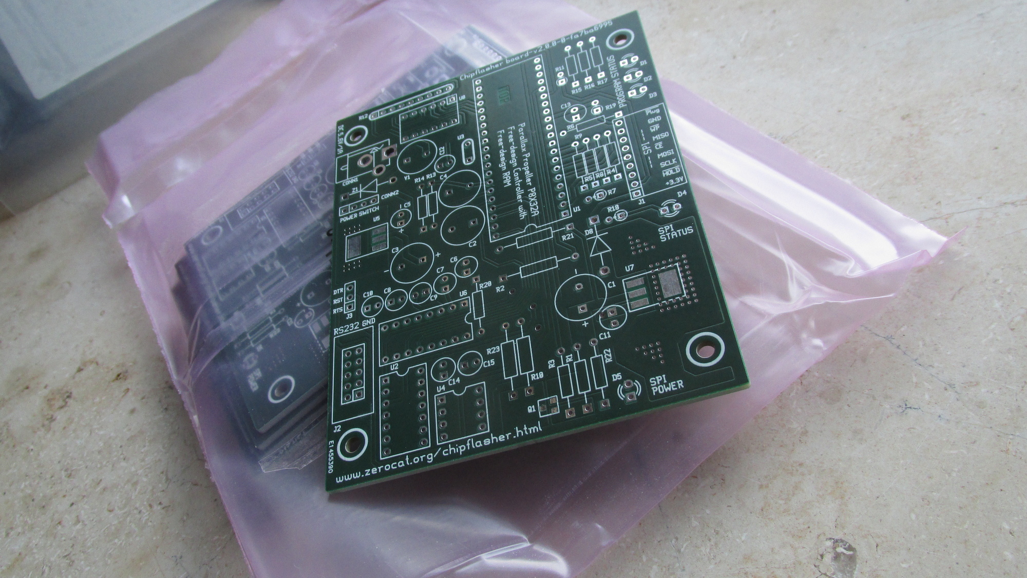
Chipflasher v2 PCB
However, this document is not a recommendation to use Eurocircuits, as their web service depends on many third party services and lots of proprietary scripts. A trial to circumvent the Google Service dependency failed as the Captcha Service cannot be avoided. :-/
Screenshots are not provided here, as website usage is bound to their terms of use: https://www.eurocircuits.com/termofuse/
    “This website contains material which is owned by or licensed to us.
    This material includes, but is not limited to, the design, layout,
    look, appearance and graphics. Reproduction is prohibited other than
    in accordance with the copyright notice, which forms part of these
    terms and conditions.”
Find the website here: https://www.eurocircuits.com/
Reduce the browser’s page display to 80%, as otherwise some buttons of their website won’t show up.
The ordering process is pretty straight forward, once you managed to create an account. Sign in/Register.
This document now should help you to fill in proper settings for their PCB-Configurator:
Go to: https://be.eurocircuits.com/shop/assembly/configurator.aspx
Select your preferred language, i.e.: English
Set Unit: Inch
Browse your disk and provide chipflasher-fa7ba6995.zip for upload.
The site will discover that standard board sizes are slightly exceeded, press OK button.
Specify/check Number of Layers: 2
Specify/check PCB size: 3.15 x 3.95 inch
Specify Delivery Format: Single PCB
Specify value for eC-registration compatible PCB: No
Stencils
Material
PCB Definition
Technology
Advanced options
Locate the button Proceed to Summary and click on it.
Summary
You can download the Basket PDF to review all details of their offer.
Enable the checkbox at the beginning of the summary line and click on Proceed to checkout.
Checkout items
All items will be listed again along with delivery address, invoice address and prices.
Now hit the final Submit button to launch the manufacturing process.
Details of the submitted order are presented for review. A technician will check all settings provided, and will contact you if things do not match.
Done! Good Luck!
    Firma
    SEGOR-electronics GmbH
    Kaiserin-Augusta-Allee 94
    10589 D-Berlin
    Telefon: +49 30 4399843
    Telefax: +49 30 4399855
    email: sales@segor.de
    Web: https://www.segor.de/
This list is meant to provide you with vendor’s part names to ease communication. Please check and verify quantities. This list might be incomplete.
    Pos.  |  Artikelbezeichnung         |  Zusatzbezeichnung            | Remark?
    ------|-----------------------------|-------------------------------|-----------
       1  |  Q  5,0 MHz-LP              |  Quarz HC49/U-S LowProfile    |
       2  |  DILLAB08                   |  Präzisionssockel DIL08       |
       3  |  DILLAB14                   |  Präzisionssockel DIL14       |
       4  |  DILLAB16                   |  Präzisionssockel DIL16       |
       5  |  DILLAB40                   |  Präzisionssockel DIL40       |
       6  |  AWHW 10/Import             |  Steckerwanne 10pol 180°      |
       7  |  DCBU 2,1-LF                |  DC-Printbuchse i=2,1mm       | x
       8  |  DCST 2,1/5,5-90°-1,5m      |  DC-Winkelstecker+Kab 1,5m    |
       9  |  SL1x40-90G                 |  Stiftl.1x40p 90°flach gew    |
      10  |  SL1x40-180G                |  Stiftl.1x40pol 180°          |
      11  |  FLLAB 1x36-180G            |  Federl.36pol 180° RM2,54     |
      12  |  USB-A ST +Kappe/sw         |  USB-A Stecker 4pol           |
      13  |  MAX 3232 CPE+              |  RS232 Transceiver DIP16      | x
      14  |  74HC  32 N                 |  Quad 2-In OR DIP14           |
      15  |  LD 1117 S33                |  V-Reg LDO 3,3V 1% SOT223     |
      16  |  24LC256 P                  |  32Kx8 I2C-EEPROM DIP8        |
      17  |  RXEF 075                   |  Multifuse Ih=0,75 It=1,5A    |
      18  |  ZD  6V8 1,3W               |  Z-Diode 6,8V 1,3W  DO41      |
      19  |  Jumper                     |  Jumper RM 2,54mm vergold.    |
      20  |  1N 4007                    |  1000V 1A Universal-Diode     |
      21  |  ELRA 100u-63/105°          |  100uF-63V 10x12,5mm RM5      |
      22  |  TA   10u-16                |  Tantal 10uF-16V 20% RM2,5    |
      23  |  1n0-R5.0-Y5P               |  1nF-100V 20% RM5             |
      24  |  IRLML 6402                 |  PMOS LL 20V 3,7A  SOT23      |
      25  |  u10-R2.5-Z5U/100x          |  100nF-50V 20% Z5U RM2,5      |
      26  |  u10-R2.5-X7R               |  100nF-50V 10% X7R RM2.5      |
      27  |  LED 3 rt-dif               |  LED 3mm rot diffus 630nm     |
      28  |  LED 3 or-dif               |  LED 3mm orange 610nm         |
      29  |  LED 3 gn-dif               |  LED 3mm grün diffus 565nm    |
      30  |  LED 3 ge-dif               |  LED 3mm gelb diffus 590nm    |
      31  |  MF 91R-1%                  |  91R 1% 0,6W/70° 0207         |
      32  |  SIL 8x 47k                 |  SIL-Netzwerk 8x47k           |
      33  |  P8X 32A-D40                |  32-Bit 80MHz 32k DIP40       |
      34  |  MF 220R-1%                 |  220R 1% 0,6W/70° 0207        |
      35  |  MF 10k-1%                  |  10k 1% 0,6W/70° 0207         |
      36  |  MF 1k0-1%                  |  1,0k 1% 0,6W/70° 0207        |
      37  |  MF 100k-1%                 |  100k 1% 0,6W/70° 0207        |
      38  |  MF 150k-1%                 |  150k 1% 0,6W/70° 0207        |
      39  |  MF 2k2-1%                  |  2,2k 1% 0,6W/70° 0207        |
      40  |  DSQ 10/rot                 |  Druckschalter 1xEIN quadr    | x
      41  |  AWP 10/Import              |  Pfostenfeldverbinder 10p.    |
      42  |  M3x25 II -8x               |  8 Abstandsbolzen M3x25mm     |
      43  |  ASH 3x15 -20x              |  20 Abstandshülsen 15mm sw    |
      44  |  M3x10 LK-100x              |  100 Linsenkopfschrauben      |
      45  |  M3x25 LK- 50x              |  50 Linsenkopfschrauben       |
      46  |  U 3,2M -100x               |  100 Unterlegscheiben 3,2     |
      47  |  ESD-Etiketten (1000x)      |  1000 Stck 37x76mm Rolle      |
      48  |  PB 0   (100x)              |  100 ESD-Beutel pink 60u      |
      49  |  Plexiglas 120x250x3        |  Acrylglas, glänzend s=3mm    | x
      50  |  DS09-POST                  |  Kabelkappe 9pol metallis.    |
      51  |  HS 152x254/Zip (100x)      |  100 ESD HighShield-Beutel    |
      52  |  MY 514 sw                  |  NF-Kabel 5x0,14mm2 schw.     |
      53  |  DS09 F                     |  Buchse  9pol Lötkelch        |
      54  |  DIP06                      |  DIP-Schalter 6-fach          | x
Position 7, DC barrel jack input, is of special significance!
This part is plugged into CONN1 location of the Chipflasher v2 PCB. The footprint has been adjusted to match this manufacturer’s part:
Manufacturer: EVE GmbH | www.eve.de
Manufacturer Part Number: DCE6A
Datasheet: https://www.eve.de/sales/document/download/filename/DCE6A.pdf
As of year 2025, this position is permanently out of stock at SEGOR. As a workaround, create yourself a drop-in replacement with SOIC MAX3232CSE+ soldered onto a tiny break-out PCB that translates SOIC pinouts towards 100.00mil grid. Add pinheaders to allow insertion into DIL16 socket.
As of 2025, this position, the main power switch, is permanently out of stock at SEGOR. As an alternative, adapt the panel cutout and try:
Position 49 is a workaround, as acrylic glass with 4mm thickness is not available.
Position 54 is an alternative drop-in replacement, RoHS-compliant, for the switch used in first chip flasher series.