|
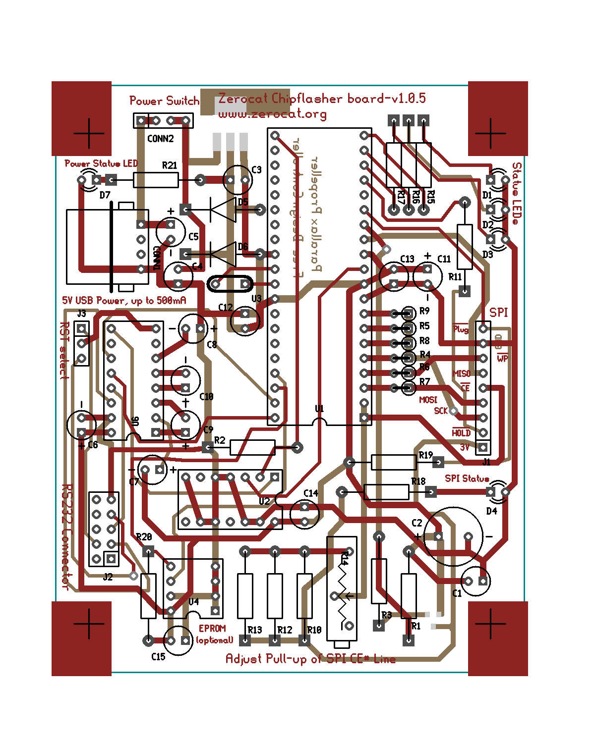
Zerocat Chipflasher Board
v0.4.3 (board-edition-1)
True Free-Design Hardware and Do-it-Yourself!
|
|
Zerocat Chipflasher Board
v0.4.3 (board-edition-1)
True Free-Design Hardware and Do-it-Yourself!
|
The PCB layout that ships with the tag pcb-prototype on branch master has been milled into copper in order to prove suitability. However, using that file for production purposes is not recommended. Several fixes were necessary.
This is a short photodocumentary of the hardware production process:
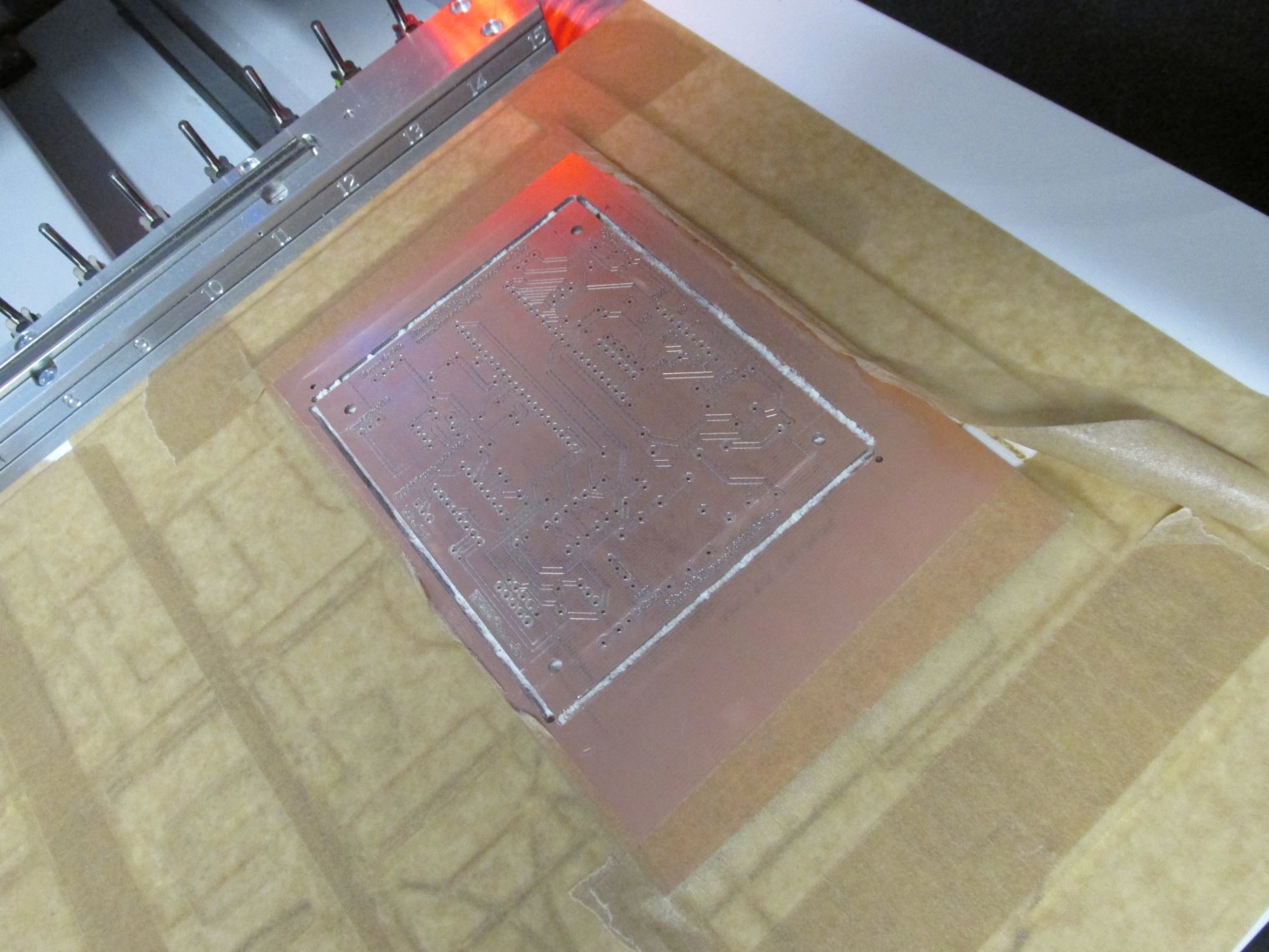
The copper board has been milled during an introductory workshop in the FABLAB Berlin.
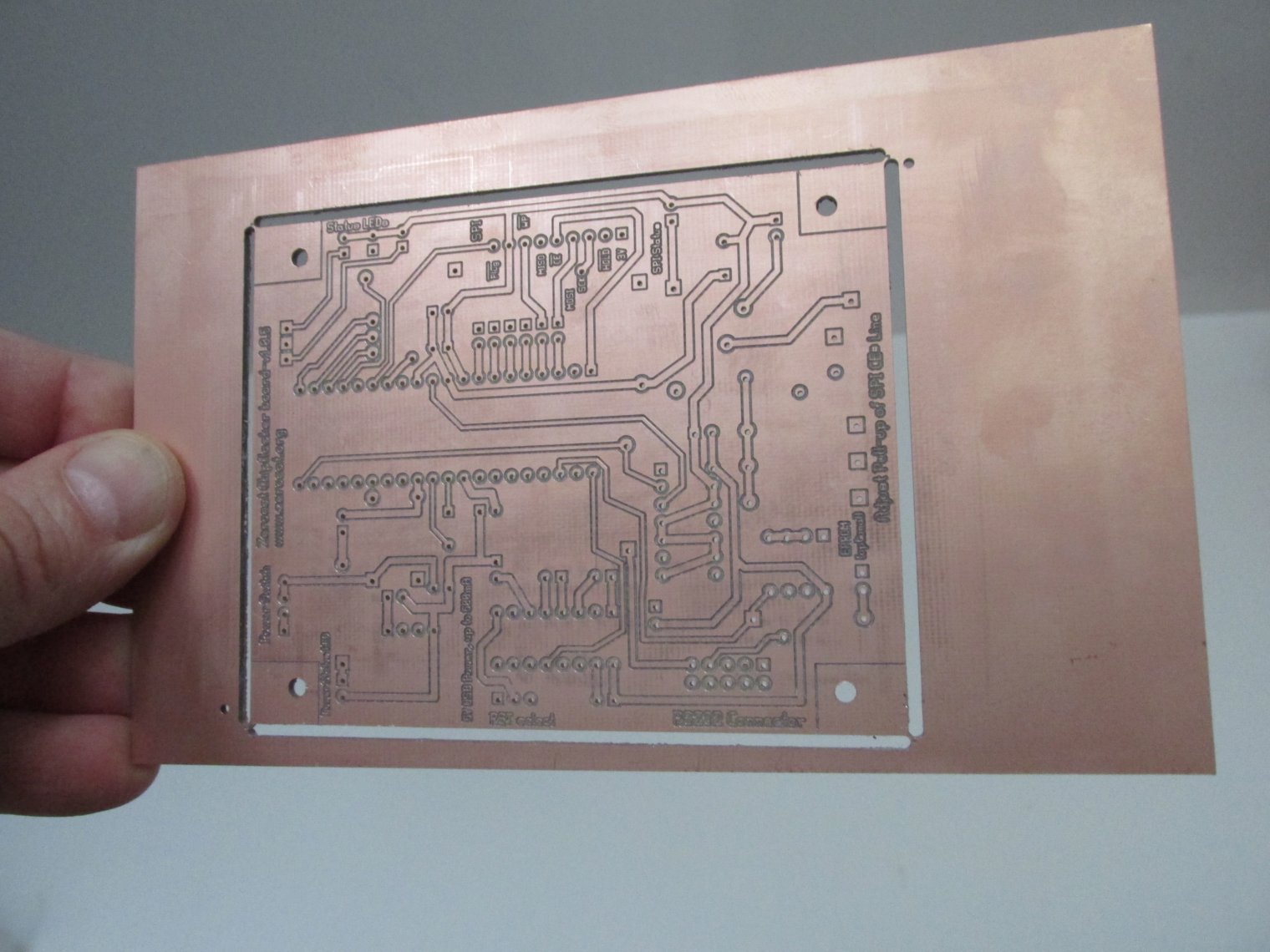
Cleaning the PCB is important, otherwise you will have to deal with dust located in the gap-routes when you want to apply clear varnish later.
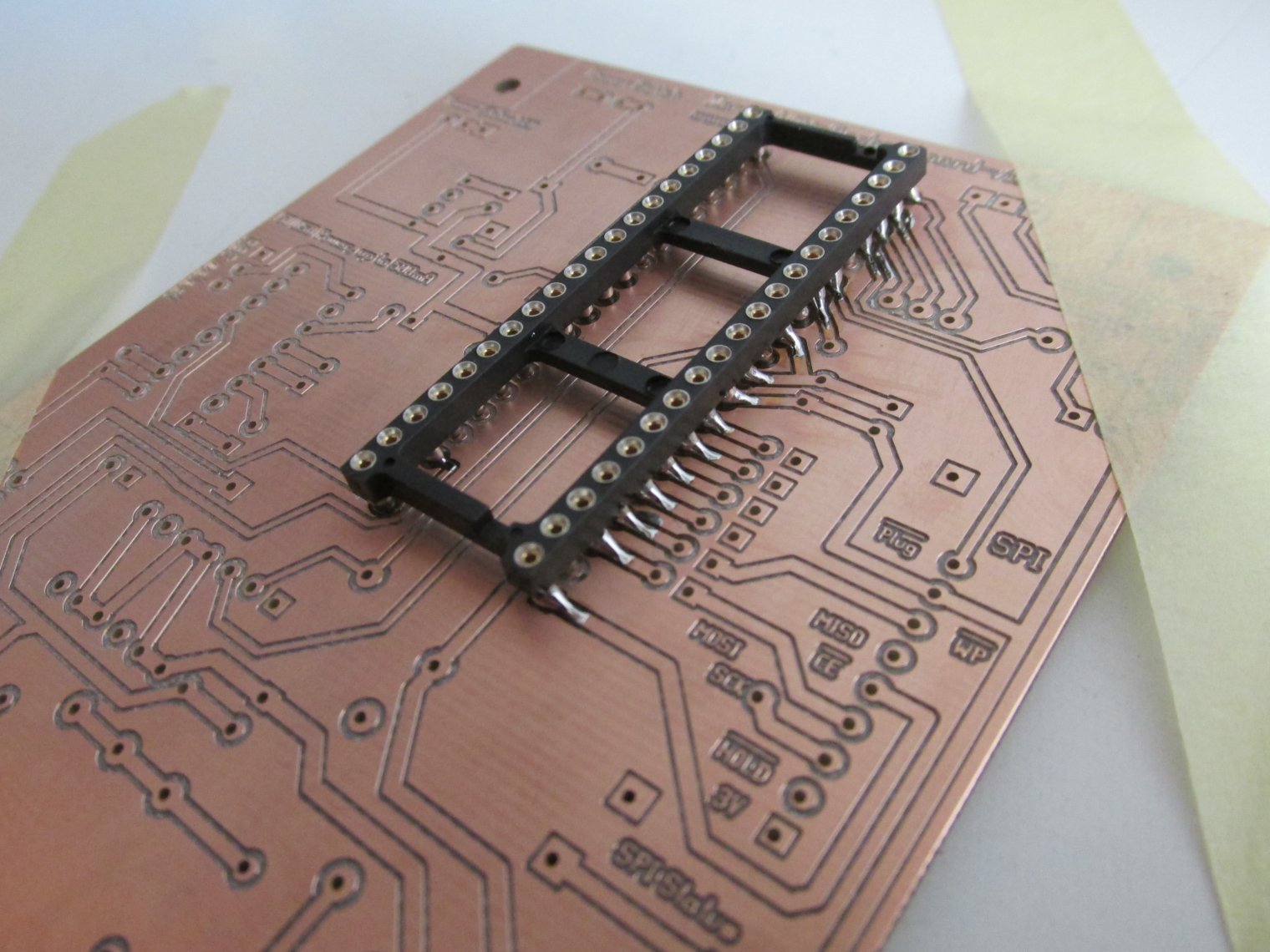
Sockets and parts with a big footprint should not to be soldered to top layer pads, this turns out to be very difficult and tricky. For example, to solder an variable resistor, you will need to use a vacuum pump while pressing the part firmly onto the surface. When done, you are lucky if the pins are still connected. And note that for some reason drilling was not always centric.
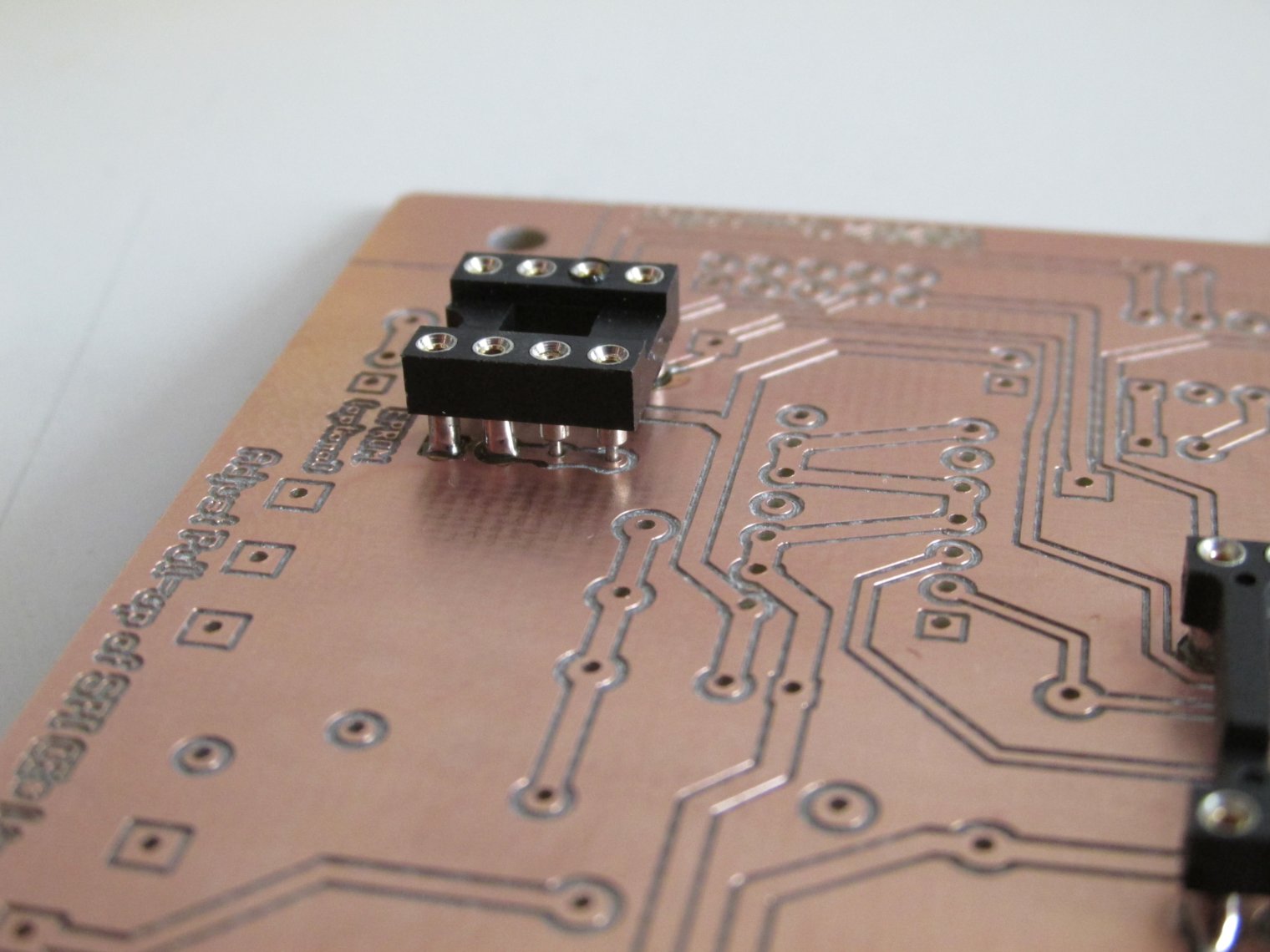
Top layer pads should be large, otherwise you will have to lever sockets or chips a bit in order to use their thin legs.
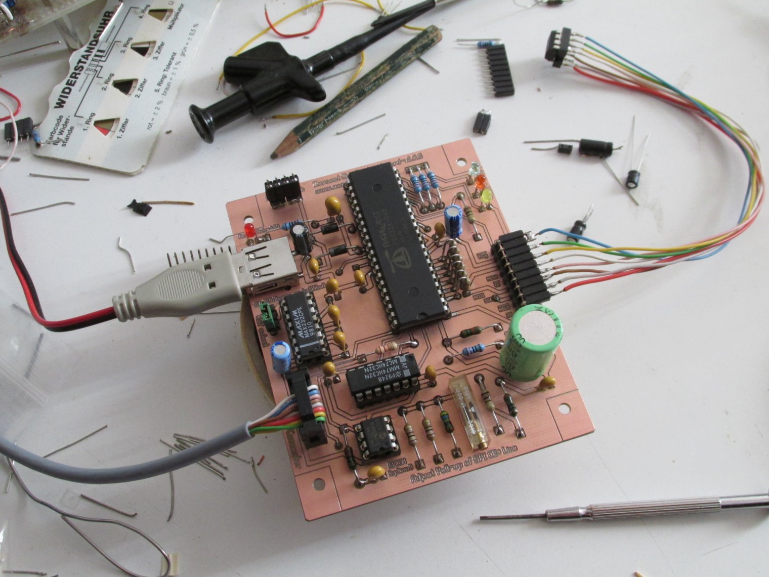
When the board is fully populated, don't forget jumpers!
Apply a clear varnish over all, but cover important contacts.
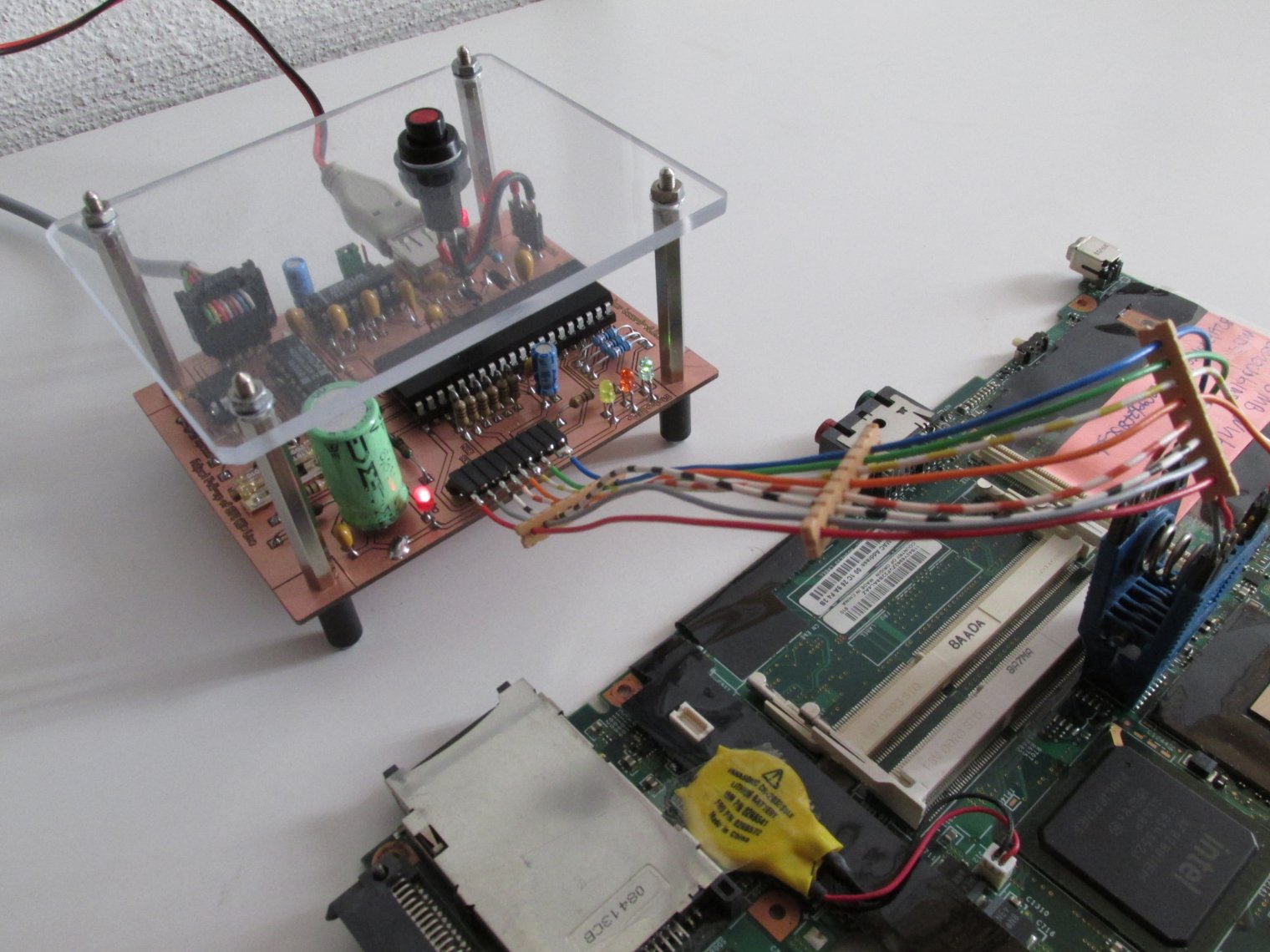
It worked right from the start. What you can see here very well is the SPI-cable which uses distances for its wires, in order to prevent signal interferences. The target shown on the photo is a T500 motherboard.
 1.8.17
Zerocat’s note on JavaScript licenses: All JavaScript files of this page are free software. Generated files (dynsections.js, menu.js, menudata.js) carry doxygen’s GNU GPLv2 license header. File jquery.js is minified code but points to corresponding source files, which in turn provide their own license infos. In case the GNU LibreJS Browser Extension complains about these scripts being non-free – please whitelist them manually and reload the page.